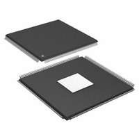
ADSP-21375KSWZ-2B Analog Devices Inc, ADSP-21375KSWZ-2B Datasheet - Page 36

ADSP-21375KSWZ-2B
Manufacturer Part Number
ADSP-21375KSWZ-2B
Description
IC DSP 32BIT 266MHZ 208-MQFP
Manufacturer
Analog Devices Inc
Series
SHARC®r
Type
Floating Pointr
Specifications of ADSP-21375KSWZ-2B
Package / Case
208-LQFP
Interface
DAI, DPI
Operating Temperature
0°C ~ 70°C
Clock Rate
266MHz
Non-volatile Memory
ROM (256 kB)
On-chip Ram
64kB
Voltage - I/o
3.30V
Voltage - Core
1.20V
Mounting Type
Surface Mount
Svhc
No SVHC (18-Jun-2010)
Base Number
21375
Core Frequency Typ
266MHz
Dsp Type
Floating Point
Mmac
532
No. Of Pins
208
Interface Type
SPI, UART
Rohs Compliant
Yes
Operating Temperature Range
0°C To +70°C
Package
208LQFP EP
Numeric And Arithmetic Format
Floating-Point
Maximum Speed
266 MHz
Ram Size
64 KB
Device Million Instructions Per Second
266 MIPS
Lead Free Status / RoHS Status
Lead free / RoHS Compliant
Available stocks
Company
Part Number
Manufacturer
Quantity
Price
Company:
Part Number:
ADSP-21375KSWZ-2B
Manufacturer:
BB
Quantity:
116
Company:
Part Number:
ADSP-21375KSWZ-2B
Manufacturer:
Analog Devices Inc
Quantity:
10 000
ADSP-21371/ADSP-21375
Parallel Data Acquisition Port (PDAP)
The timing requirements for the PDAP are provided in
Table
the IDP. For details on the operation of the PDAP, see the
PDAP chapter of the ADSP-21368 SHARC Processor Hardware
Table 34. Parallel Data Acquisition Port (PDAP)
1
Parameter
Timing Requirements
t
t
t
t
t
t
Switching Characteristics
t
t
Source pins of DATA are DATA31–12 or DAI pins. Source pins for SCLK and FS are: 1) DAI pins, 2) CLKIN through PCG, or 3) DAI pins through PCG.
SPCLKEN
HPCLKEN
PDSD
PDHD
PDCLKW
PDCLK
PDHLDD
PDSTRIB
1
1
34. PDAP is the parallel mode operation of Channel 0 of
1
1
PDAP_CLKEN Setup Before PDAP_CLK Sample Edge
PDAP_CLKEN Hold After PDAP_CLK Sample Edge
PDAP_DAT Setup Before SCLK PDAP_CLK Sample Edge
PDAP_DAT Hold After SCLK PDAP_CLK Sample Edge
Clock Width
Clock Period
Delay of PDAP Strobe After Last PDAP_CLK Capture Edge for a Word
PDAP Strobe Pulse Width
(PDAP_STROBE)
(PDAP_CLKEN)
DAI_P20
DAI_P20
(PDAP_CLK)
DAI_P20
DATA
-
-
1
-
1
1
Rev. B | Page 36 of 52 | June 2008
Figure 22. PDAP Timing
t
PDCLKW
SAMPLE EDGE
t
SPCLKEN
t
PDSD
t
PDHLDD
Reference. Note that the most significant 16 bits of external
PDAP data can be provided through the DATA31–16 pins. The
remaining four bits can only be sourced through DAI_P4–1.
The timing below is valid at the DATA31–16 pins.
t
PDCLK
t
HPCLKEN
t
PDHD
t
PDSTRB
Min
2.5
2.5
3.85
2.5
7
24
2 × t
2 × t
PCLK
PCLK
+ 3
– 1
Max
Unit
ns
ns
ns
ns
ns
ns
ns
ns


