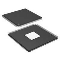
ADSP-21375KSWZ-2B Analog Devices Inc, ADSP-21375KSWZ-2B Datasheet - Page 18

ADSP-21375KSWZ-2B
Manufacturer Part Number
ADSP-21375KSWZ-2B
Description
IC DSP 32BIT 266MHZ 208-MQFP
Manufacturer
Analog Devices Inc
Series
SHARC®r
Type
Floating Pointr
Specifications of ADSP-21375KSWZ-2B
Package / Case
208-LQFP
Interface
DAI, DPI
Operating Temperature
0°C ~ 70°C
Clock Rate
266MHz
Non-volatile Memory
ROM (256 kB)
On-chip Ram
64kB
Voltage - I/o
3.30V
Voltage - Core
1.20V
Mounting Type
Surface Mount
Svhc
No SVHC (18-Jun-2010)
Base Number
21375
Core Frequency Typ
266MHz
Dsp Type
Floating Point
Mmac
532
No. Of Pins
208
Interface Type
SPI, UART
Rohs Compliant
Yes
Operating Temperature Range
0°C To +70°C
Package
208LQFP EP
Numeric And Arithmetic Format
Floating-Point
Maximum Speed
266 MHz
Ram Size
64 KB
Device Million Instructions Per Second
266 MIPS
Lead Free Status / RoHS Status
Lead free / RoHS Compliant
Available stocks
Company
Part Number
Manufacturer
Quantity
Price
Company:
Part Number:
ADSP-21375KSWZ-2B
Manufacturer:
BB
Quantity:
116
Company:
Part Number:
ADSP-21375KSWZ-2B
Manufacturer:
Analog Devices Inc
Quantity:
10 000
ADSP-21371/ADSP-21375
TIMING SPECIFICATIONS
The ADSP-21371/ADSP-21375’s internal clock (a multiple of
CLKIN) provides the clock signal for timing internal memory,
processor core, and serial ports. During reset, program the ratio
between the processor’s internal clock frequency and external
(CLKIN) clock frequency with the CLKCFG1–0 pins (see
Table 10 on Page
The ADSP-21371/ADSP-21375’s internal clock switches at
higher frequencies than the system input clock (CLKIN). To
generate the internal clock, the processor uses an internal
phase-locked loop (PLL). This PLL-based clocking minimizes
the skew between the system clock (CLKIN) signal and the pro-
cessor’s internal clock.
Core clock frequency can be calculated as:
CCLK = 1 t
CCLK
3.1 2 5M H z
66 .7M H z
CLKIN
= f
XTAL
15). To determine switching frequencies for
to
@BOOT, CLKCFG[]->PLLM[]
RESET
INPUT
(PLLM/PLLD)
AMP
÷2
00 = 6
01 = 32
10 = 16
11 = RESERVED
0
1
I NDIV[8]
Figure 3. Core Clock and System Clock Relationship to CLKIN
+
–
Rev. B | Page 18 of 52 | June 2008
4096
FILTER
LOOP
PLLM[5..0]
DELAY
÷1
CLKOUTEN[12]
M
-
CLKIN
64
MULTIPLIER
BLOCK
VCO
1 6 0 M H z < VC O_ OU T < 8 0 0M H z
the serial ports, divide down the internal clock, using the pro-
grammable divider control of each port (DIVx for the
serial ports).
Figure 3
external oscillator or crystal. Note that more ratios are possible
and can be set through software using the power management
control register (PMCTL). For more information, see the ADSP-
2136x SHARC Processor Programming Reference.
Note that in the user application, the PLL multiplier value
should be selected in such a way that the VCO frequency never
exceeds f
follows:
f
where:
PLLM = multiplier value programmed.
PLLD = divider value programmed.
f
f
f
VCO
INPUT
INPUT
INPUT
PLLD[7..6]
÷1, 2, 4, 8
= 2
= input frequency to the PLL.
= CLKIN when the input divider is disabled.
= CLKIN/2 when the input divider is enabled.
N
shows core to CLKIN ratios of 6:1, 16:1, and 32:1 with
vco
1
0
PLLM
DIVEN[9]
in
Table
1
BUFF
f
PLLBP[15]
INPUT
16. The VCO frequency is calculated as
0
1
SDRATIO[20..18]
÷2
CLKOUT
RSTO UT
CORERST
3, 3.5, 4
÷2, 2.5,
or
PCLK
(IOP)
1 00 M Hz
2 66 M Hz
CCLK
SDCLK
t o


