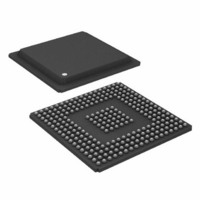
ADSP-BF535PKBZ-300 Analog Devices Inc, ADSP-BF535PKBZ-300 Datasheet - Page 17

ADSP-BF535PKBZ-300
Manufacturer Part Number
ADSP-BF535PKBZ-300
Description
IC DSP CONTROLLER 16BIT 260 BGA
Manufacturer
Analog Devices Inc
Series
Blackfin®r
Type
Fixed Pointr
Specifications of ADSP-BF535PKBZ-300
Interface
PCI, SPI, SSP, UART, USB
Clock Rate
300MHz
Non-volatile Memory
External
On-chip Ram
308kB
Voltage - I/o
3.30V
Voltage - Core
1.50V
Operating Temperature
0°C ~ 70°C
Mounting Type
Surface Mount
Package / Case
260-BGA
No. Of Bits
32 Bit
Frequency
300MHz
Supply Voltage
1.5V
Embedded Interface Type
PCI, SPI, UART
No. Of I/o's
16
Supply Voltage Range
0.95V To 1.575V, 3.15V To 3.45V
Package
260BGA
Numeric And Arithmetic Format
Floating-Point
Maximum Speed
300 MHz
Device Million Instructions Per Second
300 MIPS
Lead Free Status / RoHS Status
Lead free / RoHS Compliant
Available stocks
Company
Part Number
Manufacturer
Quantity
Price
Company:
Part Number:
ADSP-BF535PKBZ-300
Manufacturer:
Analog Devices Inc
Quantity:
10 000
PIN DESCRIPTIONS
ADSP-BF535 Blackfin processor pin definitions are listed in
Table
USB_CLK, NMI, TRST, RESET, PCI_CLK, XTALI,
XTALO.
Table 7. Pin Descriptions
REV. A
Pin
ADDR25–2
DATA31–0
ABE3–0/SDQM3–0
AMS3–0
ARDY
AOE
ARE
AWE
CLKOUT/SCLK1
SCLK0
SCKE
SA10
SRAS
SCAS
SWE
SMS3–0
TMR0
TMR1
TMR2
PF15/SPI1SEL7
PF14/SPI0SEL7
PF13/SPI1SEL6
PF12/SPI0SEL6
PF11/SPI1SEL5
PF10/SPI0SEL5
PF9/SPI1SEL4/SSEL1
PF8/SPI0SEL4/SSEL0
PF7/SPI1SEL3/DF
PF6/SPI0SEL3/MSEL6 I/O
PF5/SPI1SEL2/MSEL5 I/O
Type column symbols: G = Ground, I = Input, O = Output, P = Power supply, T = Three-state
7. The following pins are asynchronous: ARDY, PF15–0,
1
Type Function
O/T
I/O/T External data bus. (Pin has a logic-level hold circuit that prevents the input from floating
O/T
O/T
I
O/T
O
O
O
O
O/T
O/T
O/T
O/T
O/T
O/T
I/O/T Timer 0 pin. Functions as an output pin in PWMOUT mode and as an input pin in
I/O/T Timer 1 pin. Functions as an output pin in PWMOUT mode and as an input pin in
I/O/T Timer 2 pin. Functions as an output pin in PWMOUT mode and as an input pin in
I/O/T Programmable flag pin. SPI output select pin.
I/O/T Programmable flag pin. SPI output select pin.
I/O/T Programmable flag pin. SPI output select pin.
I/O/T Programmable flag pin. SPI output select pin.
I/O/T Programmable flag pin. SPI output select pin.
I/O/T Programmable flag pin. SPI output select pin (used during SPI boot).
I/O
I/O
I/O
External address bus.
internally.)
Asynchronous memory byte enables SDRAM data masks.
Chip selects for asynchronous memories.
Acknowledge signal for asynchronous memories.
Memory output enable for asynchronous memories.
Read enable for asynchronous memories.
Write enable for asynchronous memories.
SDRAM clock output pin. Same frequency and timing as SCLK0. Provided to reduce
capacitance loading on SCLK0. Connect to SDRAM’s CK pin.
SDRAM clock output pin 0. Switches at system clock frequency. Connect to the
SDRAM’s CK pin.
SDRAM clock enable pin. Connect to SDRAM’s CKE pin.
SDRAM A10 pin. SDRAM interface uses this pin to retain control of the SDRAM device
during host bus requests. Connect to SDRAM’s A10 pin.
SDRAM row address strobe pin. Connect to SDRAM’s RAS pin.
SDRAM column address select pin. Connect to SDRAM’s CAS pin.
SDRAM write enable pin. Connect to SDRAM’s WE or W buffer pin.
Memory select pin of external memory bank configured for SDRAM. Connect to
SDRAM’s chip select pin.
WIDTH_CNT and EXT_CLK modes.
WIDTH_CNT and EXT_CLK modes.
WIDTH_CNT and EXT_CLK modes.
Programmable flag pin. SPI output select pin. Sampled during reset to determine core
clock to system clock ratio.
Programmable flag pin. SPI output select pin. Sampled during reset to determine core
clock to system clock ratio.
Programmable flag pin. SPI output select pin. Sensed for configuration state during
hardware reset, used to configure the PLL. DF = 1 is for high frequency clock and divides
the input clock by 2. DF = 0 passes input clock directly to PLL phase detector.
Programmable flag pin. SPI output select pin. Sensed for configuration state during
hardware reset, used to configure the PLL. Selects CK to CLKIN ratio.
Programmable flag pin. SPI output select pin. Sensed for configuration state during
hardware reset, used to configure the PLL. Selects CK to CLKIN ratio.
–17–
ADSP-BF535


