ADSP-BF535PKBZ-300 Analog Devices Inc, ADSP-BF535PKBZ-300 Datasheet - Page 14
ADSP-BF535PKBZ-300
Manufacturer Part Number
ADSP-BF535PKBZ-300
Description
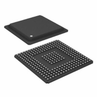
IC DSP CONTROLLER 16BIT 260 BGA
Manufacturer
Analog Devices Inc
Series
Blackfin®r
Type
Fixed Pointr
Specifications of ADSP-BF535PKBZ-300
Interface
PCI, SPI, SSP, UART, USB
Clock Rate
300MHz
Non-volatile Memory
External
On-chip Ram
308kB
Voltage - I/o
3.30V
Voltage - Core
1.50V
Operating Temperature
0°C ~ 70°C
Mounting Type
Surface Mount
Package / Case
260-BGA
No. Of Bits
32 Bit
Frequency
300MHz
Supply Voltage
1.5V
Embedded Interface Type
PCI, SPI, UART
No. Of I/o's
16
Supply Voltage Range
0.95V To 1.575V, 3.15V To 3.45V
Package
260BGA
Numeric And Arithmetic Format
Floating-Point
Maximum Speed
300 MHz
Device Million Instructions Per Second
300 MIPS
Lead Free Status / RoHS Status
Lead free / RoHS Compliant
Available stocks
Company
Part Number
Manufacturer
Quantity
Price
Company:

Part Number:
ADSP-BF535PKBZ-300
Manufacturer:
Analog Devices Inc
Quantity:
10 000


ADSP-BF535
SSEL fields define a divide ratio between the core clock (CCLK)
and the system clock.
The system clock is supplied to the CLKOUT_SCLK0 pin.
Table 5. System Clock Ratios
The maximum frequency of the system clock is f
the divisor ratio must be chosen to limit the system clock
frequency to its maximum of f
SSEL1–0 is determined by sampling the SSEL1 and SSEL0 pins
during reset. The SSEL value can be changed dynamically by
writing the appropriate values to the PLL control register
(PLL_CTL), as described in the ADSP-BF535 Blackfin Processor
Hardware Reference.
Booting Modes
The ADSP-BF535 has three mechanisms (listed in
automatically loading internal L2 memory after a reset. A fourth
mode is provided to execute from external memory, bypassing
the boot sequence.
Table 6. Booting Modes
The BMODE pins of the reset configuration register, sampled
during power-on resets and software initiated resets, implement
these modes:
Signal
Name
SSEL1– 0 CCLK/SCLK CCLK
00
01
10
11
BMODE2–0
000
001
010
011
100 –111
Execute from 16-bit external memory—Execution
starts from address 0x2000000 with 16-bit packing.
The boot ROM is bypassed in this mode.
Boot from 8-bit external flash memory—The 8-bit flash
boot routine located in boot ROM memory space is set
up using asynchronous Memory Bank 0. All configura-
tion settings are set for the slowest device possible
(3-cycle hold time; 15-cycle R/W access times; 4-cycle
setup).
Divider
Ratio
2:1
2.5:1
3:1
4:1
Description
Execute from 16-bit external memory
(Bypass Boot ROM)
Boot from 8-bit flash
Boot from SPI0 serial ROM
(8-bit address range)
Boot from SPI0 serial ROM
(16-bit address range)
Reserved
Table 5
illustrates the system clock ratios.
SCLK
Example Frequency
Ratios (MHz)
266
275
300
300
. The reset value of the
SCLK
SCLK
133
110
100
75
Table
. Note that
6) for
–14–
For each of the boot modes described above, a four-byte value is
first read from the memory device. This value is used to specify
a subsequent number of bytes to be read into the beginning of
L2 memory space. Once each of the loads is complete, the
processor jumps to the beginning of L2 space and begins
execution.
In addition, the reset configuration register can be set by appli-
cation code to bypass the normal boot sequence during a software
reset. For this case, the processor jumps directly to the beginning
of L2 memory space.
To augment the boot modes, a secondary software loader is
provided that adds additional booting mechanisms. This
secondary loader provides the capability to boot from PCI, 16-bit
flash memory, fast flash, variable baud rate, and so on.
Instruction Set Description
The Blackfin processor family assembly language instruction set
employs an algebraic syntax designed for ease of coding and read-
ability. The instructions have been specifically tuned to provide
a flexible, densely encoded instruction set that compiles to a very
small final memory size. The instruction set also provides fully
featured multifunction instructions that allow the programmer
to use many of the processor core resources in a single instruction.
Coupled with many features more often seen on microcontrol-
lers, this instruction set is very efficient when compiling C and
C++ source code. In addition, the architecture supports both a
user (algorithm/application code) and a supervisor (O/S kernel,
device drivers, debuggers, ISRs) mode of operations, allowing
multiple levels of access to core processor resources.
The assembly language, which takes advantage of the processor’s
unique architecture, offers the following advantages:
Seamlessly integrated DSP/CPU features are optimized
for both 8-bit and 16-bit operations.
A super pipelined multi issue load/store modified Harvard
architecture, which supports two 16-bit MAC or four 8-
bit ALU + two load/store + two pointer updates per cycle.
All registers, I/O, and memory are mapped into a unified
4 Gbyte memory space providing a simplified program-
ming model.
Boot from SPI serial EEPROM (8-bit addressable)—
The SPI0 uses PF10 output pin to select a single SPI
EPROM device, submits a read command at address
0x00, and begins clocking data into the beginning of L2
memory. An 8-bit addressable SPI compatible EPROM
must be used.
Boot from SPI serial EEPROM (16-bit addressable)—
The SPI0 uses PF10 output pin to select a single SPI
EPROM device, submits a read command at address
0x0000, and begins clocking data into the beginning of
L2 memory. A 16-bit addressable SPI compatible
EPROM must be used.
REV. A
Related parts for ADSP-BF535PKBZ-300
Image
Part Number
Description
Manufacturer
Datasheet
Request
R

Part Number:
Description:
±1.7g Dual-Axis IMEMS Accelerometer Evaluation Board
Manufacturer:
Analog Devices Inc
Datasheet:

Part Number:
Description:
Inertial Sensor Evaluation System
Manufacturer:
Analog Devices Inc
Datasheet:
Part Number:
Description:
Manufacturer:
Analog Devices Inc
Datasheet:
Part Number:
Description:
Manufacturer:
Analog Devices Inc
Datasheet:
Part Number:
Description:
Manufacturer:
Analog Devices Inc
Datasheet:
Part Number:
Description:
Manufacturer:
Analog Devices Inc
Datasheet:
Part Number:
Description:
Manufacturer:
Analog Devices Inc
Datasheet:
Part Number:
Description:
Manufacturer:
Analog Devices Inc
Datasheet:
Part Number:
Description:
Manufacturer:
Analog Devices Inc
Datasheet:
Part Number:
Description:
Manufacturer:
Analog Devices Inc
Datasheet:
Part Number:
Description:
Manufacturer:
Analog Devices Inc
Datasheet:
Part Number:
Description:
Manufacturer:
Analog Devices Inc
Datasheet:
Part Number:
Description:
Manufacturer:
Analog Devices Inc
Datasheet: