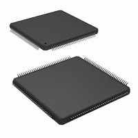
ADC083000CIYB/NOPB National Semiconductor, ADC083000CIYB/NOPB Datasheet - Page 9

ADC083000CIYB/NOPB
Manufacturer Part Number
ADC083000CIYB/NOPB
Description
IC ADC 8BIT 3GSPS LP 128-LQFP
Manufacturer
National Semiconductor
Series
PowerWise®r
Datasheet
1.ADC083000CIYBNOPB.pdf
(40 pages)
Specifications of ADC083000CIYB/NOPB
Number Of Bits
8
Sampling Rate (per Second)
3G
Data Interface
Serial
Number Of Converters
2
Power Dissipation (max)
2.3W
Voltage Supply Source
Single Supply
Operating Temperature
-40°C ~ 85°C
Mounting Type
Surface Mount
Package / Case
128-LQFP Exposed Pad
Lead Free Status / RoHS Status
Lead free / RoHS Compliant
Other names
*ADC083000CIYB
*ADC083000CIYB/NOPB
ADC083000CIYB
*ADC083000CIYB/NOPB
ADC083000CIYB
Available stocks
Company
Part Number
Manufacturer
Quantity
Price
Company:
Part Number:
ADC083000CIYB/NOPB
Manufacturer:
IPS
Quantity:
2 300
Part Number:
ADC083000CIYB/NOPB
Manufacturer:
TI/德州仪器
Quantity:
20 000
STATIC CONVERTER CHARACTERISTICS
INL
DNL
V
V
PFSE
NFSE
FS_ADJ
DYNAMIC CONVERTER CHARACTERISTICS
FPBW
ENOB
OFF
OFF
Symbol
Absolute Maximum Ratings
(Notes 1, 2)
If Military/Aerospace specified devices are required,
please contact the National Semiconductor Sales Office/
Distributors for availability and specifications.
Soldering
Semiconductor’s Reflow Temperature Profile specifications.
Refer to www.national.com/packaging. (Note 5)
Converter Electrical Characteristics
The following specifications apply after calibration for V
820mV
Non-Extended Control Mode, SDR Mode, R
bration. Boldface limits apply for T
Supply Voltage (V
Supply Difference
Voltage on Any Input Pin
(Except V
Voltage on V
(Maintaining Common Mode)
Ground Difference
Input Current at Any Pin (Note 3)
Package Input Current (Note 3)
Power Dissipation at T
ESD Susceptibility (Note 4)
Storage Temperature
_ADJ
V
|GND - DR GND|
Human Body Model
Machine Model
A
P-P
- V
, C
IN
DR
Integral Non-Linearity (Best fit)
Differential Non-Linearity
Resolution with No Missing
Codes
Offset Error
Input Offset Adjustment Range
Positive Full-Scale Error (Note 9)
Negative Full-Scale Error (Note
9)
Full-Scale Adjustment Range
Full Power Bandwidth
Word Error Rate
Gain Flatness
Effective Number of Bits
+, V
L
process
IN
= 10 pF, Differential a.c. coupled Sinewave Input Clock, f
+, V
IN
-)
A
IN
, V
-
Parameter
DR
A
must
)
≤
85°C
comply
A
−0.15V to (V
= T
MIN
−65°C to +150°C
EXT
with
-0.15V to 2.5V
to T
0V to -100mV
0V to 100 mV
DC Coupled, 1MHz Sine Wave Over
Ranged
DC Coupled, 1MHz Sine Wave Over
Ranged
Extended Control Mode
Extended Control Mode
0.0 to -1.0 dBFS
f
f
f
IN
IN
IN
= 3300Ω ±0.1%, Analog Signal Source Impedance = 100Ω Differential, after cali-
= 373 MHz, V
= 748 MHz, V
= 1498 MHz, V
A
MAX
+ 0.15V)
±25 mA
±50 mA
National
2500V
. All other limits T
2.3 W
250V
2.2V
A
= V
Conditions
DR
IN
IN
= +1.9V
9
IN
= FSR − 0.5 dB
= FSR − 0.5 dB
= FSR − 0.5 dB
Operating Ratings
Package Thermal Resistance
Ambient Temperature Range
Supply Voltage (V
Driver Supply Voltage (V
Analog Input Common Mode Voltage
V
(Maintaining Common Mode)
Ground Difference
CLK Pins Voltage Range
Differential CLK Amplitude
CLK
IN
A
DC
+, V
= 25°C, unless otherwise noted. (Notes 6, 7)
Exposed Pad
= 1.5GHz at 0.5V
(|GND - DR GND|)
, OutV = 1.9V, V
128-Lead
Package
IN
LQFP
- Voltage Range
A
)
50 to 950
(Note 8)
Typical
IN
P-P
±0.35
±0.20
−1.00
-0.20
26°C / W
10
−1.6
±45
±20
7.2
7.0
6.5
FSR (a.c. coupled) = differential
3
with 50% duty cycle, V
-18
θ
DR
JA
)
(Notes 1, 2)
(Note 8)
θ
10°C / W
Limits
Package)
JC (Top of
±0.9
±0.6
±25
±25
±15
6.8
6.6
8
−40°C
(100% duty cycle)
0.4V
(10% duty cycle)
+1.8V to +2.0V
≤
V
P-P
(Thermal Pad)
Errors/Sample
BG
2.8°C / W
0V to 2.15V
T
+1.8V to V
CMO
www.national.com
LSB (max)
LSB (max)
0V to 2.5V
θ
A
mV (max)
mV (max)
Bits (min)
Bits (min)
to 2.0V
= Floating,
(Limits)
J-PAD
≤
0V to V
Units
%FS
GHz
MHz
LSB
±50mV
Bits
Bits
mV
+85°C
0V
P-P
A
A


