ADC083000CIYB/NOPB National Semiconductor, ADC083000CIYB/NOPB Datasheet - Page 32

ADC083000CIYB/NOPB
Manufacturer Part Number
ADC083000CIYB/NOPB
Description
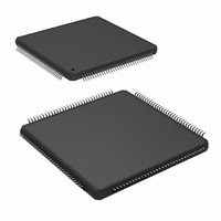
IC ADC 8BIT 3GSPS LP 128-LQFP
Manufacturer
National Semiconductor
Series
PowerWise®r
Datasheet
1.ADC083000CIYBNOPB.pdf
(40 pages)
Specifications of ADC083000CIYB/NOPB
Number Of Bits
8
Sampling Rate (per Second)
3G
Data Interface
Serial
Number Of Converters
2
Power Dissipation (max)
2.3W
Voltage Supply Source
Single Supply
Operating Temperature
-40°C ~ 85°C
Mounting Type
Surface Mount
Package / Case
128-LQFP Exposed Pad
Lead Free Status / RoHS Status
Lead free / RoHS Compliant
Other names
*ADC083000CIYB
*ADC083000CIYB/NOPB
ADC083000CIYB
*ADC083000CIYB/NOPB
ADC083000CIYB
Available stocks
Company
Part Number
Manufacturer
Quantity
Price
Company:
Part Number:
ADC083000CIYB/NOPB
Manufacturer:
IPS
Quantity:
2 300
Part Number:
ADC083000CIYB/NOPB
Manufacturer:
TI/德州仪器
Quantity:
20 000
www.national.com
lected to aid in designing the best performing single-ended to
differential conversion circuit using that particular balun.
When selecting a balun, it is important to understand the input
architecture of the ADC. There are specific balun parameters
of which the system designer should be mindful. They should
match the impedance of their analog source to the
ADC083000’s on-chip 100Ω differential input termination re-
sistor. The range of this input termination resistor is described
in the Converter Electrical Characteristics as the specification
R
Also, as a result of the ADC architecture, the phase and am-
plitude balance are important. The lowest possible phase and
amplitude imbalance is desired when selecting a balun. The
phase imbalance should be no more than ±2.5° and the am-
plitude imbalance should be limited to less than 1dB at the
desired input frequency range.
Finally, when selecting a balun, the VSWR (Voltage Standing
Wave Ratio), bandwidth and insertion loss of the balun should
also be considered. The VSWR aids in determining the overall
transmission line termination capability of the balun when in-
terfacing to the ADC input. The insertion loss should be
considered so that the signal at the balun output is within the
specified input range of the ADC as described in the Con-
verter Electrical Characteristics as the specification V
2.2.1.2 D.C. Coupled Input
When d.c. coupling to the ADC083000 analog inputs is re-
quired, single-ended to differential conversion may be easily
accomplished with the LMH6555. An example of this type of
circuit is shown in Figure 13. In such applications, the
LMH6555 performs the task of single-ended to differential
conversion while delivering low distortion and noise, as well
as output balance, that supports the operation of the
ADC083000. Connecting the ADC083000 V
V
will ensure that the common mode input voltage is as needed
for optimum performance of the ADC083000. The LMV321
was chosen to buffer V
reasonable offset voltage.
Be sure that the current drawn from the V
exceed 100 μA.
In Figure 13, R
offset that can be measured at the ADC inputs V
unadjusted positive offset with reference to V
|15mV| should be reduced with a resistor in the R
Likewise, an unadjusted negative offset with reference to
V
the R
FIGURE 13. Example of Servoing the Analog Input with
IN
CM_REF
IN-
.
greater than |15mV| should be reduced with a resistor in
ADJ+
pin of the LMH6555, through an appropriate buffer,
position. Table 7 gives suggested R
ADJ-
and R
CMO
ADJ+
V
for its low voltage operation and
are used to adjust the differential
CMO
CMO
output does not
IN-
CMO
ADJ-
ADJ-
greater than
IN+
pin to the
and R
/ V
position.
IN
20193255
IN-
.
ADJ+
. An
32
values for various unadjusted differential offsets to bring the
V
2.2.2 Out Of Range (OR) Indication
When the conversion result is clipped the Out of Range output
is activated such that OR+ goes high and OR- goes low. This
output is active as long as accurate data on either or both of
the buses would be outside the range of 00h to FFh. During
a calibration cycle, the OR output is invalid. Refer to 1.1
OVERVIEW for more details.
2.2.3 Full-Scale Input Range
As with all A/D Converters, the input range is determined by
the value of the ADC's reference voltage. The reference volt-
age of the ADC083000 is derived from an internal band-gap
reference. In the normal mode, the FSR pin controls the ef-
fective reference voltage of the ADC083000 such that the
differential full-scale input range at the analog inputs is 820
mV
low. In the Extended Control Mode, the Full Scale Range can
be set anywhere from 560mV to 840mV. Best SNR is ob-
tained with higher Full Scale Ranges, but better distortion and
SFDR are obtained with lower Full Scale Ranges. The
LMH6555 of Figure 13 is suitable for any Full Scale Range.
2.3 THE SAMPLE CLOCK INPUT
The ADC083000 has a differential LVDS clock input, CLK+ /
CLK-, which must be driven with an a.c. coupled, differential
clock signal. Although the ADC083000 is tested and its per-
formance is guaranteed with a differential 1.5 GHz clock, it
typically will function well with input clock frequencies indicat-
ed in the Electrical Characteristics Table. The clock inputs are
internally terminated and biased. The input clock signal must
be capacitively coupled to the clock pins as indicated in Figure
14.
Operation up to the sample rates indicated in the Electrical
Characteristics Table is typically possible if the maximum am-
bient temperatures indicated are not exceeded. Operating at
higher sample rates than indicated for the given ambient tem-
perature may result in reduced device reliability and product
lifetime. This is because of the higher power consumption and
die temperatures at high sample rates. Important also for re-
liability is proper thermal management . See Section 2.6.2.
IN+
P-P
/ V
Unadjusted Offset
with the FSR pin high, or is 600 mV
91mV to 110mV
IN-
TABLE 7. D.C. Coupled Offset Adjustment
11mV to 30mV
31mV to 50mV
51mV to 70mV
71mV to 90mV
0mV to 10mV
offset back to within |15mV|.
Reading
no resistor needed
Resistor Value
20.0kΩ
10.0kΩ
6.81kΩ
4.75kΩ
3.92kΩ
P-P
with FSR pin


