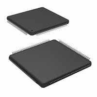
ADC083000CIYB/NOPB National Semiconductor, ADC083000CIYB/NOPB Datasheet - Page 4

ADC083000CIYB/NOPB
Manufacturer Part Number
ADC083000CIYB/NOPB
Description
IC ADC 8BIT 3GSPS LP 128-LQFP
Manufacturer
National Semiconductor
Series
PowerWise®r
Datasheet
1.ADC083000CIYBNOPB.pdf
(40 pages)
Specifications of ADC083000CIYB/NOPB
Number Of Bits
8
Sampling Rate (per Second)
3G
Data Interface
Serial
Number Of Converters
2
Power Dissipation (max)
2.3W
Voltage Supply Source
Single Supply
Operating Temperature
-40°C ~ 85°C
Mounting Type
Surface Mount
Package / Case
128-LQFP Exposed Pad
Lead Free Status / RoHS Status
Lead free / RoHS Compliant
Other names
*ADC083000CIYB
*ADC083000CIYB/NOPB
ADC083000CIYB
*ADC083000CIYB/NOPB
ADC083000CIYB
Available stocks
Company
Part Number
Manufacturer
Quantity
Price
Company:
Part Number:
ADC083000CIYB/NOPB
Manufacturer:
IPS
Quantity:
2 300
Part Number:
ADC083000CIYB/NOPB
Manufacturer:
TI/德州仪器
Quantity:
20 000
www.national.com
Pin Functions
Pin Descriptions and Equivalent Circuits
Pin No.
15
26
30
14
3
4
OutEdge / DDR /
OutV / SCLK
DCLK_RST
FSR/ECE
Symbol
SDATA
CAL
PD
Equivalent Circuit
4
Output Voltage Amplitude / Serial Interface Clock
(Input):LVCMOS Tie this pin high for normal differential DCLK
and data amplitude. Ground this pin for a reduced differential
output amplitude and reduced power consumption. See Section
1.1.6. When the extended control mode is enabled, this pin
functions as the SCLK input which clocks in the serial data. See
Section 1.2 for details on the extended control mode. See
Section 1.3 for description of the serial interface.
Edge Select / Double Data Rate / Serial Data
(Input):LVCMOS This input sets the output edge of DCLK+ at
which the output data transitions. (See Section 1.1.5.2). When
this pin is floating or connected to 1/2 the supply voltage, DDR
clocking is enabled. When the extended control mode is enabled,
this pin functions as the SDATA input. See Section 1.2 for details
on the extended control mode. See Section 1.3 for description of
the serial interface.
DCLK Reset
(Input):LVCMOS A positive pulse on this pin is used to reset
and synchronize the DCLK outs of multiple converters. See
Section 1.5 for detailed description. When bit 14 in the
Configuration Register (address 1h) is set to 0b, this single-
ended DCLK_RST pin is selected. See also pins 22,23
description.
Power Down
(Input):LVCMOS A logic high on the PD pin puts the entire
device into the Power Down Mode.
Calibration Cycle Initiate
(Input):LVCMOS A minimum 80 input clock cycles logic low
followed by a minimum of 80 input clock cycles high on this pin
initiates the calibration sequence. See Section 2.4.2 for an
overview of self-calibration and Section 2.4.2.2 for a description
of on-command calibration.
Full Scale Range Select / Extended Control Enable
(Input):LVCMOS In non-extended control mode, a logic low on
this pin sets the full-scale differential input range to 600 mV
A logic high on this pin sets the full-scale differential input range
to 820 mV
mode, whereby the serial interface and control registers are
employed, allow this pin to float or connect it to a voltage equal
to V
mode.
A
/2. See Section 1.2 for information on the extended control
P-P
. See Section 1.1.4. To enable the extended control
Description
P-P
.


