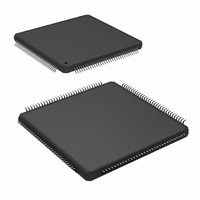
ADC08D500CIYB/NOPB National Semiconductor, ADC08D500CIYB/NOPB Datasheet - Page 36

ADC08D500CIYB/NOPB
Manufacturer Part Number
ADC08D500CIYB/NOPB
Description
IC ADC 8BIT 500MSPS DUAL 128LQFP
Manufacturer
National Semiconductor
Series
PowerWise®r
Specifications of ADC08D500CIYB/NOPB
Number Of Bits
8
Sampling Rate (per Second)
500M
Data Interface
Serial
Number Of Converters
2
Power Dissipation (max)
1.78W
Voltage Supply Source
Single Supply
Operating Temperature
-40°C ~ 85°C
Mounting Type
Surface Mount
Package / Case
128-LQFP Exposed Pad
Lead Free Status / RoHS Status
Lead free / RoHS Compliant
Other names
*ADC08D500CIYB
*ADC08D500CIYB/NOPB
ADC08D500CIYB
*ADC08D500CIYB/NOPB
ADC08D500CIYB
Available stocks
Company
Part Number
Manufacturer
Quantity
Price
Company:
Part Number:
ADC08D500CIYB/NOPB
Manufacturer:
Texas Instruments
Quantity:
10 000
www.national.com
2.0 Applications Information
Input common mode voltage must remain within 50 mV of
the V
that must also be tracked. Distortion performance will be
degraded if the input common mode voltage is more than 50
mV from V
Using an inadequate amplifier to drive the analog input.
Use care when choosing a high frequency amplifier to drive
the ADC08D500 as many high speed amplifiers will have
higher distortion than will the ADC08D500, resulting in over-
all system performance degradation.
Driving the V
mentioned in Section 2.1, the reference voltage is intended
to be fixed to provide one of two different full-scale values
(650 mV
change the full scale value, but can otherwise upset opera-
tion.
(Continued)
CMO
P-P
output , which has a variability with temperature
CMO
and 870 mV
BG
.
pin to change the reference voltage. As
P-P
). Over driving this pin will not
36
Driving the clock input with an excessively high level
signal. The ADC clock level should not exceed the level
described in the Operating Ratings Table or the input offset
could change.
Inadequate clock levels. As described in Section 2.3, insuf-
ficient clock levels can result in poor performance. Excessive
clock levels could result in the introduction of an input offset.
Using a clock source with excessive jitter, using an
excessively long clock signal trace, or having other
signals coupled to the clock signal trace. This will cause
the sampling interval to vary, causing excessive output noise
and a reduction in SNR performance.
Failure to provide adequate heat removal. As described in
Section 2.6.2, it is important to provide adequate heat re-
moval to ensure device reliability. This can either be done
with adequate air flow or the use of a simple heat sink built
into the board. The backside pad should be grounded for
best performance.


