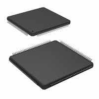
ADC08D500CIYB/NOPB National Semiconductor, ADC08D500CIYB/NOPB Datasheet - Page 11

ADC08D500CIYB/NOPB
Manufacturer Part Number
ADC08D500CIYB/NOPB
Description
IC ADC 8BIT 500MSPS DUAL 128LQFP
Manufacturer
National Semiconductor
Series
PowerWise®r
Specifications of ADC08D500CIYB/NOPB
Number Of Bits
8
Sampling Rate (per Second)
500M
Data Interface
Serial
Number Of Converters
2
Power Dissipation (max)
1.78W
Voltage Supply Source
Single Supply
Operating Temperature
-40°C ~ 85°C
Mounting Type
Surface Mount
Package / Case
128-LQFP Exposed Pad
Lead Free Status / RoHS Status
Lead free / RoHS Compliant
Other names
*ADC08D500CIYB
*ADC08D500CIYB/NOPB
ADC08D500CIYB
*ADC08D500CIYB/NOPB
ADC08D500CIYB
Available stocks
Company
Part Number
Manufacturer
Quantity
Price
Company:
Part Number:
ADC08D500CIYB/NOPB
Manufacturer:
Texas Instruments
Quantity:
10 000
AC ELECTRICAL CHARACTERISTICS
t
t
t
t
t
t
t
t
t
t
t
t
t
f
t
t
t
t
t
t
RS
RH
SD
RPW
LHT
HLT
OSK
SU
H
AD
AJ
OD
WU
SCLK
SSU
SH
CAL
CAL_L
CAL_H
CalDly
Symbol
Converter Electrical Characteristics
The following specifications apply after calibration for V
870mV
Floating, Non-Extended Control Mode, SDR Mode, R
tial. Boldface limits apply for T
P-P
, C
DCLK Duty Cycle
Reset Setup Time
Reset Hold Time
Syncronizing Edge to DCLK Output
Delay
Reset Pulse Width
Differential Low to High Transition
Time
Differential High to Low Transition
Time
DCLK to Data Output Skew
Data to DCLK Set-Up Time
DCLK to Data Hold Time
Sampling (Aperture) Delay
Aperture Jitter
Input Clock to Data Output Delay
(in addition to Pipeline Delay)
Pipeline Delay (Latency)
(Notes 11, 14)
Over Range Recovery Time
PD low to Rated Accuracy
Conversion (Wake-Up Time)
Serial Clock Frequency
Data to Serial Clock Setup Time
Data to Serial Clock Hold Time
Serial Clock Low Time
Serial Clock High Time
Calibration Cycle Time
CAL Pin Low Time
CAL Pin High Time
Calibration delay determined by pin
127
L
= 10 pF, Differential, a.c. coupled Sinewave Input Clock, f
Parameter
A
= T
MIN
to T
MAX
(Note 12)
(Note 12)
(Note 12)
f
f
(Note 11)
10% to 90%, C
10% to 90%, C
50% of DCLK transition to 50% of
Data transition, SDR Mode
and DDR Mode, 0˚ DCLK (Note 12)
DDR Mode, 90˚ DCLK (Note 12)
DDR Mode, 90˚ DCLK (Note 12)
Input CLK+ Fall to Acquisition of
Data
50% of Input Clock transition to
50% of Data transition
DI Outputs
DId Outputs
DQ Outputs
DQd Outputs
Differential V
0V to get accurate conversion
(Note 12)
(Note 12)
(Note 12)
See Figure 9 (Note 11)
See Figure 9 (Note 11)
See Section 1.1.1, Figure 9, (Note
15)
CLKIN
CLKIN
. All other limits T
EXT
= 500 MHz
= 200 MHz
A
= V
= 3300Ω
DR
Conditions
IN
(Continued)
11
L
L
step from
= +1.9V
= 2.5 pF
= 2.5 pF
±
A
0.1%, Analog Signal Source Impedance = 100Ω Differen-
= 25˚C, unless otherwise noted. (Notes 6, 7)
Normal Mode
DES Mode
Normal Mode
DES Mode
DC
CLK
±
, OutV = 1.9V, V
1.2V to
= 500 MHz at 0.5V
1.4 x 10
(Note 8)
Typical
3.53
3.85
±
150
250
250
250
500
100
IN
1.3
0.4
3.1
2.5
50
2
2
1
1
50
FSR (a.c. coupled) = differential
P-P
5
with 50% duty cycle, V
(Note 8)
Limits
13.5
14.5
2
45
55
13
14
13
14
80
80
4
4
4
25
Clock Cycles
Clock Cycles
Clock Cycles
Clock Cycles
Clock Cycles
Clock Cycles
Input Clock
www.national.com
ps (max)
% (max)
ns (min)
ns (min)
ns (min)
ns (min)
(Limits)
% (min)
ps rms
Units
Cycle
(min)
(min)
(min)
(min)
MHz
ps
ps
ns
ps
ps
ns
ns
ns
ns
ns
BG
=


