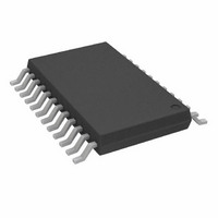
AD7192BRUZ Analog Devices Inc, AD7192BRUZ Datasheet - Page 37

AD7192BRUZ
Manufacturer Part Number
AD7192BRUZ
Description
IC ADC 24BIT 2CH W/PGA 24-TSSOP
Manufacturer
Analog Devices Inc
Datasheet
1.AD7192BRUZ.pdf
(40 pages)
Specifications of AD7192BRUZ
Data Interface
DSP, MICROWIRE™, QSPI™, Serial, SPI™
Design Resources
Precision Weigh Scale Design Using AD7192 with Internal PGA (CN0119)
Number Of Bits
24
Sampling Rate (per Second)
4.8k
Number Of Converters
1
Voltage Supply Source
Analog and Digital
Operating Temperature
-40°C ~ 105°C
Mounting Type
Surface Mount
Package / Case
24-TSSOP (0.173", 4.40mm Width)
Resolution (bits)
24bit
Input Channel Type
Pseudo Differential
Supply Voltage Range - Analogue
3V To 5.25V
Supply Voltage Range - Digital
2.7V To 5.25V
Supply
RoHS Compliant
Sampling Rate
4.8kSPS
Rohs Compliant
Yes
Lead Free Status / RoHS Status
Lead free / RoHS Compliant
Available stocks
Company
Part Number
Manufacturer
Quantity
Price
Company:
Part Number:
AD7192BRUZ
Manufacturer:
ADI
Quantity:
1 000
Company:
Part Number:
AD7192BRUZ
Manufacturer:
AD
Quantity:
1 831
Company:
Part Number:
AD7192BRUZ
Manufacturer:
ADI
Quantity:
325
Part Number:
AD7192BRUZ
Manufacturer:
ADI/亚德诺
Quantity:
20 000
Company:
Part Number:
AD7192BRUZ-REEL
Manufacturer:
ADI
Quantity:
1 000
APPLICATIONS INFORMATION
The AD7192 provides a low-cost, high resolution analog-to-
digital function. Because the analog-to-digital function is
provided by a Σ-Δ architecture, the part is more immune to
noisy environments, making it ideal for use in sensor
measurement and industrial and process control applications.
WEIGH SCALES
Figure 32 shows the AD7192 being used in a weigh scale
application. The load cell is arranged in a bridge network and
gives a differential output voltage between its OUT+ and OUT–
terminals. Assuming a 5 V excitation voltage, the full-scale
output range from the transducer is 10 mV when the sensitivity
is 2 mV/V. The excitation voltage for the bridge can be used to
directly provide the reference for the ADC because the reference
input range includes the supply voltage.
A second advantage of using the AD7192 in transducer-based
applications is that the bridge power-down switch can be fully
utilized to minimize the power consumption of the system. The
bridge power-down switch is connected in series with the cold
side of the bridge. In normal operation, the switch is closed and
OUT–
IN+
IN–
5V
OUT+
REFIN1(–)
BPDSW
REFIN1(+)
AIN1
AIN2
AIN3
AIN4
AINCOM
AGND
MUX
AGND
Figure 32. Typical Application (Weigh Scale)
AGND
AV
DD
AV
AD7192
DD
Rev. A | Page 37 of 40
SENSOR
TEMP
PGA
MCLK1 MCLK2
CIRCUITRY
measurements can be taken. In applications in which current
consumption is being minimized, the AD7192 can be placed in
standby mode, thus significantly reducing the power consumed
in the application. In addition, the bridge power-down switch
can be opened while in standby mode, thus avoiding unnecessary
power consumption by the front-end transducer. When the part
is taken out of standby mode and the bridge power-down switch
is closed, the user should ensure that the front end circuitry is
fully settled before attempting a read from the AD7192.
For simplicity, external filters are not included in Figure 32.
However, an R-C antialias filter must be included on each
analog input. This is required because the on-chip digital filter
does not provide any rejection around the modulator sampling
frequency or multiples of this frequency. Suitable values are a
100 Ω resistor in series with each analog input, a 0.1 μF
capacitor between the analog input pins, and a 0.01 μF
capacitor from each analog input pin to AGND.
CLOCK
DV
ADC
Σ-Δ
DD
DGND
P0/REFIN2(–) P1/REFIN2(+)
INTERFACE
CONTROL
SERIAL
LOGIC
REFERENCE
AND
DETECT
DOUT/RDY
DIN
SCLK
CS
SYNC
P3
P2
AD7192


