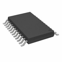
AD7192BRUZ Analog Devices Inc, AD7192BRUZ Datasheet - Page 29

AD7192BRUZ
Manufacturer Part Number
AD7192BRUZ
Description
IC ADC 24BIT 2CH W/PGA 24-TSSOP
Manufacturer
Analog Devices Inc
Datasheet
1.AD7192BRUZ.pdf
(40 pages)
Specifications of AD7192BRUZ
Data Interface
DSP, MICROWIRE™, QSPI™, Serial, SPI™
Design Resources
Precision Weigh Scale Design Using AD7192 with Internal PGA (CN0119)
Number Of Bits
24
Sampling Rate (per Second)
4.8k
Number Of Converters
1
Voltage Supply Source
Analog and Digital
Operating Temperature
-40°C ~ 105°C
Mounting Type
Surface Mount
Package / Case
24-TSSOP (0.173", 4.40mm Width)
Resolution (bits)
24bit
Input Channel Type
Pseudo Differential
Supply Voltage Range - Analogue
3V To 5.25V
Supply Voltage Range - Digital
2.7V To 5.25V
Supply
RoHS Compliant
Sampling Rate
4.8kSPS
Rohs Compliant
Yes
Lead Free Status / RoHS Status
Lead free / RoHS Compliant
Available stocks
Company
Part Number
Manufacturer
Quantity
Price
Company:
Part Number:
AD7192BRUZ
Manufacturer:
ADI
Quantity:
1 000
Company:
Part Number:
AD7192BRUZ
Manufacturer:
AD
Quantity:
1 831
Company:
Part Number:
AD7192BRUZ
Manufacturer:
ADI
Quantity:
325
Part Number:
AD7192BRUZ
Manufacturer:
ADI/亚德诺
Quantity:
20 000
Company:
Part Number:
AD7192BRUZ-REEL
Manufacturer:
ADI
Quantity:
1 000
line returns high after the first read operation. However, care
must be taken to ensure that the read operations are completed
before the next output update occurs. In continuous read mode,
the data register can be read only once.
The serial interface can operate in 3-wire mode by tying CS low.
In this case, the SCLK, DIN, and DOUT/ RDY lines are used to
communicate with the AD7192. The end of the conversion can be
monitored using the RDY bit or pin. This scheme is suitable for
interfacing to microcontrollers. If CS is required as a decoding
signal, it can be generated from a port pin. For microcontroller
interfaces, it is recommended that SCLK idle high between data
transfers.
The AD7192 can be operated with CS used as a frame synchro-
nization signal. This scheme is useful for DSP interfaces. In this
case, the first bit (MSB) is effectively clocked out by CS because
CS normally occurs after the falling edge of SCLK in DSPs. The
SCLK can continue to run between data transfers, provided the
timing numbers are obeyed.
The serial interface can be reset by writing a series of 1s to the
DIN input. If a Logic 1 is written to the AD7192 DIN line for at
least 40 serial clock cycles, the serial interface is reset. This
ensures that the interface can be reset to a known state if the
interface gets lost due to a software error or some glitch in the
system. Reset returns the interface to the state in which it expects
a write to the communications register. This operation resets the
contents of all registers to their power-on values. Following a
reset, the user should allow a period of 500 μs before addressing
the serial interface.
The AD7192 can be configured to continuously convert or to
perform a single conversion (see Figure 29 through Figure 31).
DOUT/RDY
SCLK
DIN
CS
0x08
0x280060
Figure 29. Single Conversion
Rev. A | Page 29 of 40
Single Conversion Mode
In single conversion mode, the AD7192 is placed in power-
down mode after conversions. When a single conversion is
initiated by setting MD2, MD1, and MD0 to 0, 0, 1, respectively,
in the mode register, the AD7192 powers up, performs a single
conversion, and then returns to power-down mode. The on-
chip oscillator requires 1 ms, approximately, to power up.
DOUT/ RDY goes low to indicate the completion of a conver-
sion. When the data-word has been read from the data register,
DOUT/ RDY goes high. If CS is low, DOUT/ RDY remains high
until another conversion is initiated and completed. The data
register can be read several times, if required, even when
DOUT/ RDY has gone high.
If several channels are enabled, the ADC sequences through the
enabled channels and performs a conversion on each channel.
When a conversion is started, DOUT/ RDY goes high and
remains high until a valid conversion is available. As soon as the
conversion is available, DOUT/ RDY goes low. The ADC then
selects the next channel and begins a conversion. The user can
read the present conversion while the next conversion is being
performed. As soon as the next conversion is complete, the data
register is updated; therefore, the user has a limited period in
which to read the conversion. When the ADC has performed a
single conversion on each of the selected channels, it returns to
power-down mode.
If the DAT_STA bit in the mode register is set to 1, the contents
of the status register are output along with the conversion each
time that the data read is performed. The four LSBs of the status
register indicate the channel to which the conversion corresponds.
0x58
DATA
AD7192


