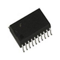
74ACT715SCNL Fairchild Semiconductor, 74ACT715SCNL Datasheet - Page 2

74ACT715SCNL
Manufacturer Part Number
74ACT715SCNL
Description
Manufacturer
Fairchild Semiconductor
Datasheet
1.74ACT715SCNL.pdf
(18 pages)
Specifications of 74ACT715SCNL
Lead Free Status / RoHS Status
Compliant
©1988 Fairchild Semiconductor Corporation
74ACT715, 74ACT715-R Rev. 1.3
Connection Diagram
Pin Description
There are a Total of 13 inputs and 5 outputs on the
ACT715.
Data Inputs D0–D7: The Data Input pins connect to the
Address Register and the Data Input Register.
ADDR/DATA: The ADDR/DATA signal is latched into
the device on the falling edge of the LOAD signal. The
signal determines if an address (0) or data (1) is present
on the data bus.
L/HBYTE: The L/HBYTE signal is latched into the device
on the falling edge of the LOAD signal. The signal deter-
mines if data will be read into the 8 LSB's (0) or the
4 MSB's (1) of the Data Registers. A 1 on this pin when
an ADDR/DATA is a 0 enables Auto-Load Mode.
LOAD: The LOAD control pin loads data into the
Address or Data Registers on the rising edge. ADDR/
DATA and L/HBYTE data is loaded into the device on
the falling edge of the LOAD. The LOAD pin has been
implemented as a Schmitt trigger input for better noise
immunity.
CLOCK: System CLOCK input from which all timing is
derived. The clock pin has been implemented as a
Schmitt trigger for better noise immunity. The CLOCK
and the LOAD signal are asynchronous and indepen-
dent. Output state changes occur on the falling edge of
CLOCK.
2
CLR: The CLEAR pin is an asynchronous input that ini-
tializes the device when it is HIGH. Initialization consists
of setting all registers to their mask programmed values,
and initializing all counters, comparators and registers.
The CLEAR pin has been implemented as a Schmitt
trigger for better noise immunity. A CLEAR pulse should
be asserted by the user immediately after power-up to
ensure proper initialization of the registers—even if the
user plans to (re)program the device.
Note: A CLEAR pulse will disable the CLOCK on the ACT715
and will enable the CLOCK on the ACT715-R.
ODD/EVEN: Output that identifies if display is in odd
(HIGH) or even (LOW) field of interlace when device is in
interlaced mode of operation. In noninterlaced mode of
operation this output is always HIGH. Data can be seri-
ally scanned out on this pin during Scan Mode.
VCSYNC: Outputs Vertical or Composite Sync signal
based on value of the Status Register. Equalization and
Serration pulses will (if enabled) be output on the
VCSYNC signal in composite mode only.
VCBLANK: Outputs Vertical or Composite Blanking
signal based on value of the Status Register.
HBLHDR: Outputs Horizontal Blanking signal, Horizon-
tal Gating signal or Cursor Position based on value of
the Status Register.
HSYNVDR: Outputs Horizontal Sync signal, Vertical
Gating signal or Vertical Interrupt signal based on value
of Status Register.
www.fairchildsemi.com


