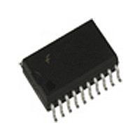
74ACT715SCNL Fairchild Semiconductor, 74ACT715SCNL Datasheet

74ACT715SCNL
Specifications of 74ACT715SCNL
Related parts for 74ACT715SCNL
74ACT715SCNL Summary of contents
Page 1
... M20B 74ACT715-RSC M20B Device also available in Tape and Reel. Specify by appending suffix letter “X” to the ordering number. FACT™ trademark of Fairchild Semiconductor Corporation. ©1988 Fairchild Semiconductor Corporation 74ACT715, 74ACT715-R Rev. 1.3 General Description The ACT715 and ACT715-R are 20-pin TTL-input ...
Page 2
... LOAD signal are asynchronous and indepen- dent. Output state changes occur on the falling edge of CLOCK. ©1988 Fairchild Semiconductor Corporation 74ACT715, 74ACT715-R Rev. 1.3 CLR: The CLEAR pin is an asynchronous input that ini- tializes the device when it is HIGH. Initialization consists of setting all registers to their mask programmed values, and initializing all counters, comparators and registers ...
Page 3
... Logic Block Diagram ©1988 Fairchild Semiconductor Corporation 74ACT715, 74ACT715-R Rev. 1.3 Figure 1. 3 www.fairchildsemi.com ...
Page 4
... Supply Voltage CC V Input Voltage I V Output Voltage O T Operating Temperature A ∆ ∆ t Minimum Input Edge Rate: V from 0.8V to 2.0V ©1988 Fairchild Semiconductor Corporation 74ACT715, 74ACT715-R Rev. 1.3 Parameter Parameter @ 4.5V, 5. Rating –0.5V to +7.0V –20mA +20mA –0. 0.5V CC –20mA +20mA –0. ...
Page 5
... B5— VCBLANK Polarity B6— VCSYNC Polarity B7— HBLHDR Polarity B8— HSYNVDR Polarity ©1988 Fairchild Semiconductor Corporation 74ACT715, 74ACT715-R Rev. 1.3 Bits 9–11 Bits 9 through 11 enable several different features of the device. B9— Enable Equalization/Serration Pulses (0) Disable Equalization/Serration Pulses (1) B10— Disable System Clock (0) Enable System Clock (1) Default values for B10 are “ ...
Page 6
... In non-interlaced mode, all vertical timing is based on whole-lines. Register 8 is ©1988 Fairchild Semiconductor Corporation 74ACT715, 74ACT715-R Rev. 1.3 always based on whole-lines and does not add 1 for the first clock. The vertical counter starts at the value of 1 and counts until the value of VMAX ...
Page 7
... Figure 4. Equalization/Serration Interval Programming ©1988 Fairchild Semiconductor Corporation 74ACT715, 74ACT715-R Rev. 1.3 Figure 2. Horizontal Wave Specification Figure 3. Vertical Waveform Specification 7 www.fairchildsemi.com ...
Page 8
... In the auto load sequence the low order byte of the data register will be written first followed by the high order byte on the next load cycle. At the time the High ©1988 Fairchild Semiconductor Corporation 74ACT715, 74ACT715-R Rev. 1.3 Cursor Position and Vertical Interrupt ...
Page 9
... Enable Hbyte Data Load 4 Enable Lbyte Data Load 5 Enable Hbyte Data Load 6 Enable Manual Addressing ©1988 Fairchild Semiconductor Corporation 74ACT715, 74ACT715-R Rev. 1.3 Load Falling Edge Load Falling Edge Load Start Address n Load Lbyte (n) Load Hbyte (n); Inc Counter Load Lbyte (n+1) Load Hbyte (n+1) ...
Page 10
... Data or Status Registers. This address is read into the device in a similar fashion as all of the other registers the ©1988 Fairchild Semiconductor Corporation 74ACT715, 74ACT715-R Rev. 1.3 ADDRDATA pin (Auto Addressing Mode) will not cause this address to automatically increment ...
Page 11
... REG14 REG15 REG16 REG17 REG18 ©1988 Fairchild Semiconductor Corporation 74ACT715, 74ACT715-R Rev. 1.3 Normal device operation can be resumed by loading in a non-scan address. As the scanning of the registers is a non-destructive scan, the device will resume correct operation from the point at which it was halted. ...
Page 12
... RS170 Verticle Data Signal VFP VSYNC Width VBLANK Width 20 Lines VDRIVE Width 11.0 Lines VEQP Intrvl VPERiod (field) 262.5 Lines VPERiod (frame) 525 Lines ©1988 Fairchild Semiconductor Corporation 74ACT715, 74ACT715-R Rev. 1.3 Width µs 1.536 4.749 10.895 6.356 2.375 4.749 63.556 Width µs 3 Lines 190 ...
Page 13
... ODD) f Non-Interlaced f MAX MAX (HMAX/2 is EVEN Clock to Any Output PLH1 PHL1 Clock to ODDEVEN PLH2 PHL2 (Scan Mode) t Load to Outputs PLH3 ©1988 Fairchild Semiconductor Corporation 74ACT715, 74ACT715-R Rev. 1.3 = +25° (V) Conditions Typ 0.1V 4.5 V 1.5 OUT or V – 0.1V 5.5 1 ...
Page 14
... CLR Pulse Width HIGH wclr t CLOCK Pulse Width wck (HIGH or LOW) Note: 3. Removal of Vectored Reset or Restart to Clock. Capacitance Symbol Parameter C Input Capacitance IN C Power Dissipation Capacitance PD ©1988 Fairchild Semiconductor Corporation 74ACT715, 74ACT715-R Rev. 1.3 = +25° (V) Typ. Guaranteed Minimums CC 5.0 3.0 4.0 3.0 4.0 5.0 2 ...
Page 15
... CLK. The end of the signals will occur as programmed. At the completion of the first frame, the signals will resume to their programmed start and end time. ©1988 Fairchild Semiconductor Corporation 74ACT715, 74ACT715-R Rev. 1.3 Preprogramming “On-the-Fly” Although the ACT715 and ACT715-R are completely programmable, certain limitations must be set as to when and how the parts can be reprogrammed ...
Page 16
... Note: A 74HC221A may be substituted for the 74HC423A Pin 6 and Pin 14 must be hardwired to GND Components R1: 4.7k R2: 10k Figure 8. Circuit for Clear and Load Pulse Generation ©1988 Fairchild Semiconductor Corporation 74ACT715, 74ACT715-R Rev. 1.3 C1: 10µF C2: 50pF 16 www.fairchildsemi.com ...
Page 17
... Physical Dimensions Dimensions are in inches (millimeters) unless otherwise noted. Figure 9. 20-Lead Small Outline Integrated Circuit (SOIC), JEDEC MS-013, 0.300" Wide ©1988 Fairchild Semiconductor Corporation 74ACT715, 74ACT715-R Rev. 1.3 Package Number M20B 17 www.fairchildsemi.com ...
Page 18
... TRADEMARKS The following are registered and unregistered trademarks Fairchild Semiconductor owns or is authorized to use and is not intended exhaustive list of all such trademarks. ® ACEx Across the board. Around the world. ActiveArray Bottomless Build it Now CoolFET CROSSVOLT CTL™ Current Transfer Logic™ ...


