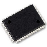
MT48LC2M32B2P-6:G Micron Technology Inc, MT48LC2M32B2P-6:G Datasheet - Page 21

MT48LC2M32B2P-6:G
Manufacturer Part Number
MT48LC2M32B2P-6:G
Description
IC, SDRAM, 64MBIT, 166MHZ, TSOP-86
Manufacturer
Micron Technology Inc
Type
SDRAMr
Series
-r
Specifications of MT48LC2M32B2P-6:G
Organization
2Mx32
Density
64Mb
Address Bus
13b
Access Time (max)
17/7.5/5.5ns
Maximum Clock Rate
166MHz
Operating Supply Voltage (typ)
3.3V
Package Type
TSOP-II
Operating Temp Range
0C to 70C
Operating Supply Voltage (max)
3.6V
Operating Supply Voltage (min)
3V
Supply Current
180mA
Pin Count
86
Mounting
Surface Mount
Operating Temperature Classification
Commercial
Memory Type
DRAM - Sychronous
Access Time
5.5ns
Page Size
64Mbit
Memory Case Style
TSOP
No. Of Pins
86
Operating Temperature Range
0°C To +70°C
Frequency
166MHz
Supply Voltage
3.3V
Format - Memory
RAM
Memory Size
64M (2Mx32)
Speed
167MHz
Interface
Parallel
Voltage - Supply
3 V ~ 3.6 V
Operating Temperature
0°C ~ 70°C
Package / Case
86-TFSOP (0.400", 10.16mm Width)
Filter Terminals
SMD
Rohs Compliant
Yes
Lead Free Status / RoHS Status
Compliant
Lead Free Status / RoHS Status
Compliant, Lead free / RoHS Compliant
Available stocks
Company
Part Number
Manufacturer
Quantity
Price
Part Number:
MT48LC2M32B2P-6:G
Manufacturer:
MICRON
Quantity:
20 000
Figure 9:
READs
PDF: 09005aef80725c0b/Source: 09005aef806fc13c
64MSDRAM_2.fm - Rev. M 10/07 EN
Example: Meeting
READ bursts are initiated with a READ command, as shown in Figure 10 on page 22.
The starting column and bank addresses are provided with the READ command, and
auto precharge is either enabled or disabled for that burst access. If auto precharge is
enabled, the row being accessed is precharged at the completion of the burst. For the
generic READ commands used in the following illustrations, auto precharge is disabled.
During READ bursts, the valid data-out element from the starting column address will
be available following the CL after the READ command. Each subsequent data-out
element will be valid by the next positive clock edge. Figure 11 on page 22 shows general
timing for each possible CL setting.
Upon completion of a burst, assuming no other commands have been initiated, the DQs
will go High-Z. A full-page burst will continue until terminated. (At the end of the page, it
will wrap to column 0 and continue.)
Data from any READ burst may be truncated with a subsequent READ command, and
data from a fixed-length READ burst may be immediately followed by data from a READ
command. In either case, a continuous flow of data can be maintained. The first data
element from the new burst follows either the last element of a completed burst or the
last desired data element of a longer burst which is being truncated.
The new READ command should be issued x cycles before the clock edge at which the
last desired data element is valid, where x = CL -1. This is shown in Figure 12 on page 23
for CL = 2 and CL = 3; data element n + 3 is either the last of a burst of four or the last
desired of a longer burst. The 64Mb SDRAM uses a pipelined architecture and therefore
does not require the 2n rule associated with a prefetch architecture. A READ command
can be initiated on any clock cycle following a previous READ command. Full-speed
random read accesses can be performed to the same bank, as shown in Figure 13 on
page 24, or each subsequent READ may be performed to a different bank.
COMMAND
CLK
t
RCD (MIN) When 2 <
ACTIVE
T0
T1
NOP
t
RCD
21
t
RCD (MIN)/
T2
NOP
Micron Technology, Inc., reserves the right to change products or specifications without notice.
t
READ or
CK ≤ 3
WRITE
T3
DON’T CARE
64Mb: x4, x8, x16 SDRAM
T4
©2000 Micron Technology, Inc. All rights reserved.
Commands


