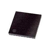
ATA5812-PLQW80 Atmel, ATA5812-PLQW80 Datasheet - Page 33

ATA5812-PLQW80
Manufacturer Part Number
ATA5812-PLQW80
Description
RF Transceiver RF Data Control Transceiver
Manufacturer
Atmel
Datasheet
1.ATA5811-PLHC.pdf
(92 pages)
Specifications of ATA5812-PLQW80
Wireless Frequency
226 KHz
Interface Type
4-Wire SPI
Noise Figure
7 dB
Output Power
10 dBm
Operating Supply Voltage
2.4 V to 5.25 V
Maximum Operating Temperature
+ 105 C
Mounting Style
SMD/SMT
Package / Case
QFN-48
Maximum Data Rate
20 Kbps
Minimum Operating Temperature
- 40 C
Modulation
ASK, FSK
Lead Free Status / RoHS Status
Lead free / RoHS Compliant
- Current page: 33 of 92
- Download datasheet (2Mb)
7.6
8. Microcontroller Interface
9. Digital Control Logic
9.1
4689F–RKE–08/06
2-Battery Application
Register Structure
The supply voltage range is 4.4V to 6.6V and VAUX is connected to an inductive supply.
Figure 7-6.
The microcontroller interface is a level converter which converts all internal digital signals which
are referred to the DVCC voltage, into the voltage used by the microcontroller. Therefore, the pin
VSINT has to be connected to the supply voltage of the microcontroller.
This makes it possible to use the internal voltage regulator/switch at pin VSOUT as in
on page 6
to the supply voltage of the microcontroller as in
The configuration of the transceiver is stored in RAM cells. The RAM contains a 16
TX/RX data buffer and a 6
interface (CS, SCK, SDI_TMDI, SDO_TMDO).
The 1
8-bit status register is not part of the RAM and is readable via the 4-wire serial interface.
and
2-Battery Application with Inductive Emergency Supply
Figure 4-1 on page 8
RF-Transceiver
Digital Control
Logic
ATA5811/ATA5812
SDO_TMDO
8-bit control register and is write and readable via a 4-wire serial
DEM_OUT
SDI_TMDI
NRESET
VSOUT
VSINT
AVCC
DVCC
VAUX
SCK
CLK
VS1
VS2
IRQ
CS
or to connect the microcontroller and the pin VSINT directly
Figure 3-1 on page
4.4V to 6.6V
ATA5811/ATA5812
VS
OUT
OUT
OUT
IN
IN
IN
IN
Microcontroller
7.
Figure 2-1
8-bit
33
Related parts for ATA5812-PLQW80
Image
Part Number
Description
Manufacturer
Datasheet
Request
R

Part Number:
Description:
IC TXRX UHF ASK/FSK 1CH 48-QFN
Manufacturer:
Atmel
Datasheet:

Part Number:
Description:
Manufacturer:
Atmel
Datasheet:

Part Number:
Description:
DEV KIT FOR AVR/AVR32
Manufacturer:
Atmel
Datasheet:

Part Number:
Description:
INTERVAL AND WIPE/WASH WIPER CONTROL IC WITH DELAY
Manufacturer:
ATMEL Corporation
Datasheet:

Part Number:
Description:
Low-Voltage Voice-Switched IC for Hands-Free Operation
Manufacturer:
ATMEL Corporation
Datasheet:

Part Number:
Description:
MONOLITHIC INTEGRATED FEATUREPHONE CIRCUIT
Manufacturer:
ATMEL Corporation
Datasheet:

Part Number:
Description:
AM-FM Receiver IC U4255BM-M
Manufacturer:
ATMEL Corporation
Datasheet:

Part Number:
Description:
Monolithic Integrated Feature Phone Circuit
Manufacturer:
ATMEL Corporation
Datasheet:

Part Number:
Description:
Multistandard Video-IF and Quasi Parallel Sound Processing
Manufacturer:
ATMEL Corporation
Datasheet:

Part Number:
Description:
High-performance EE PLD
Manufacturer:
ATMEL Corporation
Datasheet:


