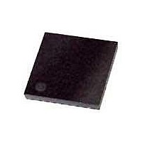
ATA5812-PLQW80 Atmel, ATA5812-PLQW80 Datasheet - Page 20

ATA5812-PLQW80
Manufacturer Part Number
ATA5812-PLQW80
Description
RF Transceiver RF Data Control Transceiver
Manufacturer
Atmel
Datasheet
1.ATA5811-PLHC.pdf
(92 pages)
Specifications of ATA5812-PLQW80
Wireless Frequency
226 KHz
Interface Type
4-Wire SPI
Noise Figure
7 dB
Output Power
10 dBm
Operating Supply Voltage
2.4 V to 5.25 V
Maximum Operating Temperature
+ 105 C
Mounting Style
SMD/SMT
Package / Case
QFN-48
Maximum Data Rate
20 Kbps
Minimum Operating Temperature
- 40 C
Modulation
ASK, FSK
Lead Free Status / RoHS Status
Lead free / RoHS Compliant
Table 5-7.
5.13
20
Frequency (MHz) TX Current (mA) Output Power (dBm) R1 (k )
433.92
433.92
433.92
868.3
868.3
868.3
315
315
315
Output Power and TX Supply Current versus Supply Voltage and Temperature
ATA5811/ATA5812
Measured Output Power and Current Consumption with VS1 = VS2 = 3 V, T
10.5
16.7
11.2
17.8
11.5
16.3
8.5
8.6
9.3
Table 5-8 on page 20
VS1 = VS2 = VS in the 433.92 MHz and 6.2 dBm case versus temperature and supply voltage
measured according to
opposed to the receiver sensitivity the supply voltage has here the major impact on output power
variations because of the large signal behavior of a power amplifier. Thus, a two battery system
with voltage regulator or a 5V system shows much less variation than a 2.4V to 3.6V one battery
system because the supply voltage is then well within 3.0V and 3.6V.
The reason is that the amplitude at the output RF_OUT with optimum load resistance is
AVCC – 0.4V and the power is proportional to (AVCC – 0.4V)
changed. This means that the theoretical output power reduction if reducing the supply voltage
from 3.0V to 2.4V is 10 log ((3V – 0.4V)
behavior in the measurement. This is not the same case for higher voltages since here increas-
ing the supply voltage from 3V to 3.6V should theoretical increase the power by 1.8 dB but only
0.8 dB in the measurement shows that the amplitude does not increase with the supply voltage
because the load impedance is optimized for 3V and the output amplitude stays more constant.
Table 5-8.
Table 5-9 on page 21
pared to 3.0V/25°C. As can be seen a temperature change to
the power by less than 1 dB due to the bandgap regulated output current. Measurements of all
the cases in
same relative behavior as shown in
T
T
T
amb
amb
amb
VS =
= +105°C
= –40°C
= +25°C
Table 5-7 on page 20
Measured Output Power and Supply Current at 433.92 MHz, PWR_H = GND
10.5
–0.3
0.4
5.7
0.1
6.2
5.4
9.5
11
shows the relative changes of the output power of a typical device com-
shows the measurement of the output power for a typical device with
Figure 5-10 on page 19
10.19 mA
10.62 mA
3.8 dBm
4.6 dBm
11.4 mA
3.8 dBm
2.4 V
56
27
27
56
22
22
33
15
22
over temperature and supply voltage have shown about the
Table 5-9 on page
2
/(2.4V – 0.4V)
VPWR_H
AVCC
AVCC
AVCC
GND
GND
GND
GND
GND
GND
with components according to
R
2
Lopt
2500
2300
1170
) = 2.2 dB.
21.
920
350
890
300
471
245
10.19 mA
11.19 mA
12.02 mA
5.5 dBm
6.2 dBm
5.4 dBm
3.0 V
( )
–
L1 (nH)
40° as well as to +105° reduces
amb
2
82
68
56
56
47
33
12
15
10
Table 5-8
if the load impedance is not
= 25°C
Q
28
32
35
40
38
43
58
54
57
L1
shows that principle
C1 (pF) C3 (pF)
10.78 mA
11.79 mA
12.73 mA
6.2 dBm
7.1 dBm
6.3 dBm
0.75
3.6 V
1.5
2.2
3.9
1.5
2.7
1.0
1.0
1.5
Table
4689F–RKE–08/06
5-7. As
3.3
0
0
0
0
0
0
0
0


