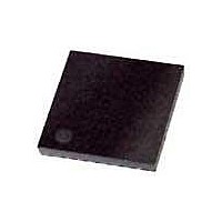
ATA5812-PLQW80 Atmel, ATA5812-PLQW80 Datasheet - Page 18

ATA5812-PLQW80
Manufacturer Part Number
ATA5812-PLQW80
Description
RF Transceiver RF Data Control Transceiver
Manufacturer
Atmel
Datasheet
1.ATA5811-PLHC.pdf
(92 pages)
Specifications of ATA5812-PLQW80
Wireless Frequency
226 KHz
Interface Type
4-Wire SPI
Noise Figure
7 dB
Output Power
10 dBm
Operating Supply Voltage
2.4 V to 5.25 V
Maximum Operating Temperature
+ 105 C
Mounting Style
SMD/SMT
Package / Case
QFN-48
Maximum Data Rate
20 Kbps
Minimum Operating Temperature
- 40 C
Modulation
ASK, FSK
Lead Free Status / RoHS Status
Lead free / RoHS Compliant
Figure 5-9.
5.12
18
Output Power Setting and PA Matching at RF_OUT
ATA5811/ATA5812
Ref 10 dBm
Samp
Log
10
dB/
VAvg
5 0
W1 S2
S3 FC
Center 433.92 MHz
Res BW 10 kHz
FSK-modulated TX Spectrum (20 Kbit/s/ 16.17 kHz/Manchester Code)
The Power Amplifier (PA) is a single-ended open collector stage which delivers a current pulse
which is nearly independent of supply voltage, temperature and tolerances due to bandgap sta-
bilization. Resistor R
current in the PA. A higher resistor value results in a lower reference current, a lower output
power and a lower current consumption of the PA. The usable range of R
PWR_H switches the output power range between about 0 dBm to 5 dBm (PWR_H = GND) and
5 dBm to 10 dBm (PWR_H = AVCC) by multiplying this reference current with a factor 1
(PWR_H = GND) and 2.5 (PWR_H = AVCC) which corresponds to about 5 dB more output
power.
If the PA is switched off in TX mode, the current consumption without output stage with
VS1 = VS2 = 3V, T
433.92 MHz.
The maximum output power is achieved with optimum load resistances R
5-7 on page 20
absorbing it into the matching network consisting of L
19. There must be also a low resistive DC path to AVCC to deliver the DC current of the power
amplifier's last stage. The matching of the PA output was done with the circuit according to
ure 5-10 on page 19
elements may be necessary to compensate for individual board layouts.
with compensation of the 1.0 pF output capacitance of the RF_OUT pin by
Atten 20 dB
amb
1
with the values in
, see
= 25°C is typically 6.5 mA for 868.3 MHz and 6.95 mA for 315 MHz and
Figure 5-10 on page
VBW 10 kHz
Table 5-7 on page
19, sets a reference current which controls the
1
, C
1
, C
20. Note that value changes of these
Sweep 27.5 ms (401 pts)
Span 1 MHz
3
as shown in
1
Lopt
is 15 k to 56 k . Pin
Figure 5-10 on page
according to
4689F–RKE–08/06
Table
Fig-


