PBR951,215 NXP Semiconductors, PBR951,215 Datasheet - Page 2
PBR951,215
Manufacturer Part Number
PBR951,215
Description
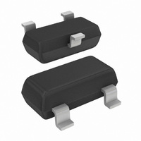
TRANSISTOR NPN UHF 100MA SOT23
Manufacturer
NXP Semiconductors
Datasheet
1.PBR951215.pdf
(16 pages)
Specifications of PBR951,215
Package / Case
SOT-23-3, TO-236-3, Micro3™, SSD3, SST3
Transistor Type
NPN
Voltage - Collector Emitter Breakdown (max)
10V
Frequency - Transition
8GHz
Noise Figure (db Typ @ F)
1.3dB ~ 2dB @ 1GHz ~ 2GHz
Power - Max
365mW
Dc Current Gain (hfe) (min) @ Ic, Vce
50 @ 5mA, 6V
Current - Collector (ic) (max)
100mA
Mounting Type
Surface Mount
Dc Current Gain Hfe Max
50 @ 5mA @ 6V
Mounting Style
SMD/SMT
Configuration
Single
Transistor Polarity
NPN
Maximum Operating Frequency
8000 MHz (Typ)
Collector- Emitter Voltage Vceo Max
10 V
Emitter- Base Voltage Vebo
1.5 V
Continuous Collector Current
0.1 A
Power Dissipation
365 mW
Maximum Operating Temperature
+ 175 C
Lead Free Status / RoHS Status
Lead free / RoHS Compliant
Gain
-
Lead Free Status / Rohs Status
Lead free / RoHS Compliant
Other names
568-1175-2
934043070215
PBR951 T/R
934043070215
PBR951 T/R


Philips Semiconductors
FEATURES
APPLICATIONS
DESCRIPTION
Silicon NPN transistor in a surface mount 3-pin SOT23
package. The transistor is primarily intended for wideband
applications in the GHz-range in the RF front end of analog
and digital cellular telephones, cordless phones, radar
detectors, pagers and satellite TV-tuners.
QUICK REFERENCE DATA
Note
1. T
1998 Aug 10
C
f
G
F
P
R
T
SYMBOL
Small size
Low noise
Low distortion
High gain
Gold metallization ensures excellent reliability.
Communication and instrumentation systems.
tot
re
th j-s
UHF wideband transistor
UM
s
is the temperature at the soldering point of the collector pin.
feedback capacitance
transition frequency
maximum unilateral power gain
noise figure
total power dissipation
thermal resistance from junction to
soldering point
PARAMETER
I
I
I
f = 1 GHz
f = 1 GHz
T
P
C
C
C
S
s
tot
= 0; V
= 30 mA; V
= 30 mA; V
= 60 C; note 1
=
= 365 mW
opt
2
CB
; I
PINNING - SOT23
handbook, halfpage
C
= 6 V; f = 1 MHz
CONDITIONS
PIN
Marking code: W2.
= 5 mA; V
1
2
3
CE
CE
Top view
= 6 V; f
= 6 V; T
Fig.1 Simplified outline and symbol.
base
emitter
collector
CE
m
1
amb
= 6 V;
= 1 GHz
= 25 C;
3
DESCRIPTION
2
0.4
8
14
1.3
TYP.
MAM255
Product specification
1
365
315
MAX.
PBR951
3
2
pF
GHz
dB
dB
mW
K/W
UNIT
Related parts for PBR951,215
Image
Part Number
Description
Manufacturer
Datasheet
Request
R

Part Number:
Description:
Uhf Wideband Transistor
Manufacturer:
NXP Semiconductors
Datasheet:
Part Number:
Description:
NXP Semiconductors designed the LPC2420/2460 microcontroller around a 16-bit/32-bitARM7TDMI-S CPU core with real-time debug interfaces that include both JTAG andembedded trace
Manufacturer:
NXP Semiconductors
Datasheet:

Part Number:
Description:
NXP Semiconductors designed the LPC2458 microcontroller around a 16-bit/32-bitARM7TDMI-S CPU core with real-time debug interfaces that include both JTAG andembedded trace
Manufacturer:
NXP Semiconductors
Datasheet:
Part Number:
Description:
NXP Semiconductors designed the LPC2468 microcontroller around a 16-bit/32-bitARM7TDMI-S CPU core with real-time debug interfaces that include both JTAG andembedded trace
Manufacturer:
NXP Semiconductors
Datasheet:
Part Number:
Description:
NXP Semiconductors designed the LPC2470 microcontroller, powered by theARM7TDMI-S core, to be a highly integrated microcontroller for a wide range ofapplications that require advanced communications and high quality graphic displays
Manufacturer:
NXP Semiconductors
Datasheet:
Part Number:
Description:
NXP Semiconductors designed the LPC2478 microcontroller, powered by theARM7TDMI-S core, to be a highly integrated microcontroller for a wide range ofapplications that require advanced communications and high quality graphic displays
Manufacturer:
NXP Semiconductors
Datasheet:
Part Number:
Description:
The Philips Semiconductors XA (eXtended Architecture) family of 16-bit single-chip microcontrollers is powerful enough to easily handle the requirements of high performance embedded applications, yet inexpensive enough to compete in the market for hi
Manufacturer:
NXP Semiconductors
Datasheet:
Part Number:
Description:
The XA-S3 device is a member of Philips Semiconductors? XA(eXtended Architecture) family of high performance 16-bitsingle-chip microcontrollers
Manufacturer:
NXP Semiconductors
Datasheet:

Part Number:
Description:
The NXP BlueStreak LH75401/LH75411 family consists of two low-cost 16/32-bit System-on-Chip (SoC) devices
Manufacturer:
NXP Semiconductors
Datasheet:
Part Number:
Description:
The NXP LPC3130/3131 combine an 180 MHz ARM926EJ-S CPU core, high-speed USB2
Manufacturer:
NXP Semiconductors
Datasheet:
Part Number:
Description:
The NXP LPC3141 combine a 270 MHz ARM926EJ-S CPU core, High-speed USB 2
Manufacturer:
NXP Semiconductors
Part Number:
Description:
The NXP LPC3143 combine a 270 MHz ARM926EJ-S CPU core, High-speed USB 2
Manufacturer:
NXP Semiconductors

Part Number:
Description:
The NXP LPC3152 combines an 180 MHz ARM926EJ-S CPU core, High-speed USB 2
Manufacturer:
NXP Semiconductors
Part Number:
Description:
The NXP LPC3154 combines an 180 MHz ARM926EJ-S CPU core, High-speed USB 2
Manufacturer:
NXP Semiconductors