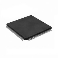
CY7C0851AV-133AXI Cypress Semiconductor Corp, CY7C0851AV-133AXI Datasheet - Page 14

CY7C0851AV-133AXI
Manufacturer Part Number
CY7C0851AV-133AXI
Description
CY7C0851AV-133AXI
Manufacturer
Cypress Semiconductor Corp
Datasheet
1.CY7C0851AV-133AXI.pdf
(36 pages)
Specifications of CY7C0851AV-133AXI
Format - Memory
RAM
Memory Type
SRAM - Dual Port, Synchronous
Memory Size
2M (64K x 36)
Speed
133MHz
Interface
Parallel
Voltage - Supply
3.135 V ~ 3.465 V
Operating Temperature
-40°C ~ 85°C
Package / Case
176-LQFP
Lead Free Status / RoHS Status
Lead free / RoHS Compliant
Available stocks
Company
Part Number
Manufacturer
Quantity
Price
Company:
Part Number:
CY7C0851AV-133AXI
Manufacturer:
Cypress Semiconductor Corp
Quantity:
10 000
Maximum Ratings
Exceeding maximum ratings
device. These user guidelines are not tested.
Storage temperature............................... –65
Ambient temperature with
Power applied.......................................... –55
Supply voltage to ground potential ..............–0.5 V to + 4.6 V
DC voltage applied to
Outputs in High-Z state........................ –0.5 V to V
Electrical Characteristics
Over the Operating Range
Capacitance
Notes
Document #: 38-06070 Rev. *J
V
V
V
V
I
I
I
I
I
I
I
I
I
CY7C0850AV,CY7C0851V
CY7C0851AV, CY7C0852V,
CY7C0852AV
CY7C0853V,CY7C0853AV
Parameter
19. The voltage on any input or I/O pin can not exceed the power pin during power up.
20. Pulse width < 20 ns.
21. C
22. I
OZ
IX1
IX2
CC
SB1
SB2
SB3
SB4
SB5
OH
OL
IH
IL
SB1
[22]
[22]
[22]
[22]
OUT
Part Number
, I
SB2
also references C
, I
SB3
Output HIGH voltage (V
Output LOW voltage (V
Input HIGH voltage
Input LOW voltage
Output leakage current
Input leakage current except TDI, TMS, MRST
Input leakage current TDI, TMS, MRST
Operating current for
(V
Outputs disabled
Standby current (both ports TTL level)
CE
Standby current (one port TTL level)
CE
Standby current (both ports CMOS level)
CE
Standby current (one port CMOS level)
CE
Operating current
(V
Outputs disabled
DD
DD
and I
L
L
L
L
and CE
| CE
and CE
| CE
= Max.,I
= Max, I
SB4
[21]
I/O
R
R
are not applicable forCY7C0853V/ CY7C0853AV because it can not be powered down by using chip enable pins.
.
V
V
R
R
OUT
OUT
V
V
IH
IH
[19]
, f = f
, f = f
C
C
C
C
IH
DD
= 0 mA),
= 0 mA, f = 0)
Parameter
IN
OUT
IN
OUT
may impair the useful life of the
Description
, f = f
– 0.2 V, f = 0
MAX
MAX
DD
DD
MAX
= Min., I
= Min., I
Input capacitance
Output capacitance
Input capacitance
Output capacitance
CY7C0850AV
CY7C0851V/AV
CY7C0852V/AV
CY7C0853V/
CY7C0853AV
CY7C0853V/
CY7C0853AV
C to + 150
C to + 125
OL
OH
Description
DD
= +4.0 mA)
= –4.0 mA)
+ 0.5 V
C
C
–0.1
Min
–10
–10
2.4
2.0
CY7C0850AV,CY7C0851V/CY7C0851AV
T
V
–
–
–
–
–
–
–
–
–
A
DD
DC input voltage ............................. –0.5 V to V
Output current into outputs (LOW) .............................. 20 mA
Static discharge voltage........................................... > 2000 V
(JEDEC JESD22-A114-2000B)
Latch-up current ..................................................... > 200 mA
Operating Range
Commercial
Industrial
= 25
= 3.3 V
Typ
-167
225
160
160
90
55
–
–
–
Test Conditions
Range
C, f = 1 MHz,
Max
300
115
210
210
0.4
1.0
0.8
10
10
75
–
–
–
–
–0.1
Min
–10
–10
2.4
2.0
–
–
–
–
–
–
–
–
–
Ambient Temperature
CY7C0852V/CY7C0852AV
CY7C0853V/CY7C0853AV
–40
0
-133
Typ
225
270
160
160
90
55
70
–
–
–
C to +70
C to +85
Max
300
400
115
210
210
100
0.4
0.8
1.0
10
10
75
–
–
Max
13
10
22
20
C
–0.1
C
Min
–10
–10
2.4
2.0
–
–
–
–
–
–
–
-100
Typ
200
160
160
90
55
70
3.3 V ± 165 mV
3.3 V ± 165 mV
–
–
–
–
DD
Page 14 of 36
+ 0.5 V
V
Max
310
210
210
100
115
0.4
0.8
1.0
Unit
10
10
75
DD
pF
pF
pF
pF
–
–
–
[20]
Unit
mA
mA
mA
mA
mA
mA
mA
A
A
V
V
V
V
[+] Feedback


