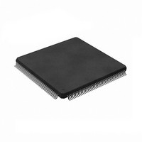
CY7C0851AV-133AXI Cypress Semiconductor Corp, CY7C0851AV-133AXI Datasheet - Page 10

CY7C0851AV-133AXI
Manufacturer Part Number
CY7C0851AV-133AXI
Description
CY7C0851AV-133AXI
Manufacturer
Cypress Semiconductor Corp
Datasheet
1.CY7C0851AV-133AXI.pdf
(36 pages)
Specifications of CY7C0851AV-133AXI
Format - Memory
RAM
Memory Type
SRAM - Dual Port, Synchronous
Memory Size
2M (64K x 36)
Speed
133MHz
Interface
Parallel
Voltage - Supply
3.135 V ~ 3.465 V
Operating Temperature
-40°C ~ 85°C
Package / Case
176-LQFP
Lead Free Status / RoHS Status
Lead free / RoHS Compliant
Available stocks
Company
Part Number
Manufacturer
Quantity
Price
Company:
Part Number:
CY7C0851AV-133AXI
Manufacturer:
Cypress Semiconductor Corp
Quantity:
10 000
Counter Interrupt
The counter interrupt (CNTINT) is asserted LOW when an
increment operation results in the unmasked portion of the
counter register being all “1s.” It is deasserted HIGH when an
Increment operation results in any other value. It is also
de-asserted by Counter Reset, Counter Load, Mask Reset and
Mask Load operations, and by MRST.
Retransmit
Retransmit is a feature that allows the Read of a block of memory
more than once without the need to reload the initial address.
This eliminates the need for external logic to store and route
data. It also reduces the complexity of the system design and
saves board space. An internal “mirror register” is used to store
the initially loaded address counter value. When the counter
unmasked portion reaches its maximum value set by the mask
register, it wraps back to the initial value stored in this “mirror
register.” If the counter is continuously configured in increment
mode, it increments again to its maximum value and wraps back
to the value initially stored into the “mirror register.” Thus, the
repeated access of the same data is allowed without the need
for any external logic.
Mask Reset Operation
The mask register is reset to all “1s,” which unmasks every bit of
the counter. Master reset (MRST) also resets the mask register
to all “1s.”
Document #: 38-06070 Rev. *J
CY7C0850AV,CY7C0851V/CY7C0851AV
Mask Load Operation
The mask register is loaded with the address value presented at
the address lines. Not all values permit correct increment
operations. Permitted values are of the form 2
From the most significant bit to the least significant bit, permitted
values have zero or more “0s,” one or more “1s,” or one “0.” Thus
1FFFF, 003FE, and 00001 are permitted values, but 1F0FF,
003FC, and 00000 are not.
Mask Readback Operation
The internal value of the mask register can be read out on the
address lines. Readback is pipelined; the address is valid t
after the next rising edge of the port’s clock. If mask readback
occurs while the port is enabled (CE0 LOW and CE1 HIGH), the
data lines (DQs) is three-stated.
block diagram of the operation.
Counting by Two
When the least significant bit of the mask register is “0,” the
counter increments by two. This may be used to connect the
CY7C0850AV/CY7C0851V/0851AV/CY7C0852V/CY7C0852AV
as a 72-bit single port SRAM in which the counter of one port
counts even addresses and the counter of the other port counts
odd addresses. This even-odd address scheme stores one half
of the 72-bit data in even memory locations, and the other half in
odd memory locations.
CY7C0852V/CY7C0852AV
CY7C0853V/CY7C0853AV
Figure 4 on page 11
n
– 1 or 2
Page 10 of 36
shows a
n
– 2.
CM2
[+] Feedback


