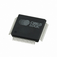
CS42888-CQZ Cirrus Logic Inc, CS42888-CQZ Datasheet - Page 34

CS42888-CQZ
Manufacturer Part Number
CS42888-CQZ
Description
IC,Soundcard Circuits,CMOS,QFP,64PIN,PLASTIC
Manufacturer
Cirrus Logic Inc
Type
Audio Codecr
Datasheet
1.CS42888-CQZR.pdf
(61 pages)
Specifications of CS42888-CQZ
Data Interface
Serial
Resolution (bits)
24 b
Number Of Adcs / Dacs
4 / 8
Sigma Delta
Yes
Dynamic Range, Adcs / Dacs (db) Typ
105 / 108 (Differential), 102 / 105 (Single-Ended)
Voltage - Supply, Analog
3.14 V ~ 5.25 V
Voltage - Supply, Digital
3.14 V ~ 5.25 V
Operating Temperature
-10°C ~ 70°C
Mounting Type
Surface Mount
Package / Case
64-LQFP
No. Of Adcs
2
No. Of Dacs
4
No. Of Input Channels
8
No. Of Output Channels
4
Adc / Dac Resolution
24bit
Ic Interface Type
Serial
Supply Voltage Range
3.14V To 5.25V
Lead Free Status / RoHS Status
Lead free / RoHS Compliant
Other names
598-1183
Available stocks
Company
Part Number
Manufacturer
Quantity
Price
Company:
Part Number:
CS42888-CQZ
Manufacturer:
Cirrus Logic Inc
Quantity:
10 000
Company:
Part Number:
CS42888-CQZR
Manufacturer:
Cirrus Logic Inc
Quantity:
10 000
34
4.7.1
4.7.2
C C L K
CS
C D IN
C D O U T
SPI Mode
In SPI Mode, CS is the CS42888 chip-select signal, CCLK is the control port bit clock (input into the
CS42888 from the microcontroller), CDIN is the input data line from the microcontroller, CDOUT is the
output data line to the microcontroller. Data is clocked in on the rising edge of CCLK and out on the falling
edge.
Figure 22
first seven bits on CDIN form the chip address and must be 1001111. The eighth bit is a read/write indi-
cator (R/W), which should be low to write. The next eight bits form the Memory Address Pointer (MAP),
which is set to the address of the register that is to be updated. The next eight bits are the data which will
be placed into the register designated by the MAP. During writes, the CDOUT output stays in the Hi-Z
state. It may be externally pulled high or low with a 47 kΩ resistor, if desired.
There is a MAP auto-increment capability, enabled by the INCR bit in the MAP register. If INCR is a zero,
the MAP will stay constant for successive read or writes. If INCR is set to a 1, the MAP will auto-increment
after each byte is read or written, allowing block reads or writes of successive registers.
To read a register, the MAP has to be set to the correct address by executing a partial write cycle which
finishes (CS high) immediately after the MAP byte. The MAP auto-increment bit (INCR) may be set or not,
as desired. To begin a read, bring CS low, send out the chip address and set the read/write bit (R/W) high.
The next falling edge of CCLK will clock out the MSB of the addressed register (CDOUT will leave the high
impedance state). If the MAP auto-increment bit is set to 1, the data for successive registers will appear
consecutively.
I²C Mode
In I²C Mode, SDA is a bidirectional data line. Data is clocked into and out of the part by the clock, SCL.
There is no CS pin. Pins AD0 and AD1 form the two least-significant bits of the chip address and should
be connected through a resistor to VLC or DGND as desired. The state of the pins is sensed while the
CS42888 is being reset.
The signal timings for a read and write cycle are shown in
defined as a falling transition of SDA while the clock is high. A Stop condition is a rising transition while
the clock is high. All other transitions of SDA occur while the clock is low. The first byte sent to the
CS42888 after a Start condition consists of a 7-bit chip address field and a R/W bit (high for a read, low
for a write). The upper 5 bits of the 7-bit address field are fixed at 10010. To communicate with a CS42888,
the chip address field, which is the first byte sent to the CS42888, should match 10010 followed by the
settings of the AD1 and AD0. The eighth bit of the address is the R/W bit. If the operation is a write, the
ADDRESS
MAP = Memory Address Pointer, 8 bits, MSB first
1001111
C H I P
shows the operation of the control port in SPI Mode. To write to a register, bring CS low. The
High Impedance
R/W
Figure 22. Control Port Timing in SPI Mode
M A P
MSB
b y te 1
DATA
b y te n
LSB
A D D R E S S
C H IP
1001111
Figure 23
R/W
MSB
and
Figure
LSB MSB
24. A Start condition is
CS42888
LSB
DS717F2


