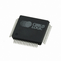
CS42888-CQZ Cirrus Logic Inc, CS42888-CQZ Datasheet - Page 25

CS42888-CQZ
Manufacturer Part Number
CS42888-CQZ
Description
IC,Soundcard Circuits,CMOS,QFP,64PIN,PLASTIC
Manufacturer
Cirrus Logic Inc
Type
Audio Codecr
Datasheet
1.CS42888-CQZR.pdf
(61 pages)
Specifications of CS42888-CQZ
Data Interface
Serial
Resolution (bits)
24 b
Number Of Adcs / Dacs
4 / 8
Sigma Delta
Yes
Dynamic Range, Adcs / Dacs (db) Typ
105 / 108 (Differential), 102 / 105 (Single-Ended)
Voltage - Supply, Analog
3.14 V ~ 5.25 V
Voltage - Supply, Digital
3.14 V ~ 5.25 V
Operating Temperature
-10°C ~ 70°C
Mounting Type
Surface Mount
Package / Case
64-LQFP
No. Of Adcs
2
No. Of Dacs
4
No. Of Input Channels
8
No. Of Output Channels
4
Adc / Dac Resolution
24bit
Ic Interface Type
Serial
Supply Voltage Range
3.14V To 5.25V
Lead Free Status / RoHS Status
Lead free / RoHS Compliant
Other names
598-1183
Available stocks
Company
Part Number
Manufacturer
Quantity
Price
Company:
Part Number:
CS42888-CQZ
Manufacturer:
Cirrus Logic Inc
Quantity:
10 000
Company:
Part Number:
CS42888-CQZR
Manufacturer:
Cirrus Logic Inc
Quantity:
10 000
DS717F2
4.2.2
4.3
4.3.1
Analog Outputs
The high-pass filter for ADC1/ADC2 can be enabled and disabled. The high-pass filters are controlled us-
ing the HPF_FREEZE bit in the register
The ADC output data is in 2’s complement binary format. For inputs above positive full scale or below neg-
ative full scale, the ADC will output 7FFFFFH or 800000H, respectively, and cause the ADC Overflow bit
in the register
High-Pass Filter and DC Offset Calibration
The high-pass filter continuously subtracts a measure of the DC offset from the output of the decimation
filter. If the high-pass filter is disabled during normal operation, the current value of the DC offset for the
corresponding channel is frozen and this DC offset will continue to be subtracted from the conversion re-
sult. This feature makes it possible to perform a system DC offset calibration by:
1. Running the CS42888 with the high-pass filter enabled until the filter settles. See the Digital Filter
2. Disabling the high-pass filter and freezing the stored DC offset.
Initialization
The initialization and Power-Down sequence flow chart is shown in
enters a power-down state upon initial power-up. The interpolation and decimation filters, delta-sigma
modulators and control port registers are reset. The internal voltage reference, multi-bit digital-to-analog
and analog-to-digital converters and switched-capacitor low-pass filters are powered down.
The device remains in the power-down state until the RST pin is brought high. The control port is acces-
sible once RST is high, and the desired register settings can be loaded per the interface descriptions in
the
VQ will quickly charge to VA/2 upon initial power up. Once MCLK is valid and the PDN bit is set to ‘0’b,
the internal voltage reference, FILT+_ADC and FILT+_DAC, will ramp up to approximately VA. Power is
applied to the D/A converters and switched-capacitor filters, and the analog outputs are clamped to the
quiescent voltage, VQ. Once LRCK is valid, MCLK occurrences are counted over one LRCK period to
determine the MCLK/LRCK frequency ratio. After an approximate 2000 sample period delay, normal op-
eration begins.
“Control Port Description and Timing” on page
Characteristics for filter settling time.
“Status (Address 19h) (Read Only)” on page 49
3.9 V
1.1 V
3.9 V
1.1 V
2.5 V
2.5 V
(AINx+) - (AINx-) = 5.6 V
Full-Scale Differential Input Level =
Figure 10. Full-Scale Input
“ADC Control & DAC De-Emphasis (Address 05h)” on page
PP
= 1.98 V
RMS
33.
AINx-
AINx+
to be set to a ‘1’.
Figure 11 on page
VA
5.0 V
26. The CS42888
CS42888
44.
25


