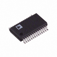
AD9220ARS Analog Devices Inc, AD9220ARS Datasheet - Page 22

AD9220ARS
Manufacturer Part Number
AD9220ARS
Description
A/D Converter (A-D) IC
Manufacturer
Analog Devices Inc
Specifications of AD9220ARS
Peak Reflow Compatible (260 C)
No
No. Of Bits
12 Bit
Leaded Process Compatible
No
Mounting Type
Surface Mount
No. Of Channels
2
Interface Type
Parallel
Package / Case
28-SSOP
Rohs Status
RoHS non-compliant
Number Of Bits
12
Sampling Rate (per Second)
10M
Data Interface
Parallel
Number Of Converters
7
Power Dissipation (max)
310mW
Voltage Supply Source
Single Supply
Operating Temperature
-40°C ~ 85°C
Number Of Elements
1
Resolution
12Bit
Architecture
Pipelined
Sample Rate
10MSPS
Input Polarity
Unipolar
Input Type
Voltage
Rated Input Volt
±1/±2.5V
Differential Input
Yes
Power Supply Requirement
Analog and Digital
Single Supply Voltage (typ)
5V
Single Supply Voltage (min)
4.75V
Single Supply Voltage (max)
5.25V
Dual Supply Voltage (typ)
Not RequiredV
Dual Supply Voltage (min)
Not RequiredV
Dual Supply Voltage (max)
Not RequiredV
Power Dissipation
310mW
Differential Linearity Error
±0.75LSB
Integral Nonlinearity Error
±1.25LSB
Operating Temp Range
-40C to 85C
Operating Temperature Classification
Industrial
Mounting
Surface Mount
Pin Count
28
Package Type
SSOP
Lead Free Status / RoHS Status
Contains lead / RoHS non-compliant
For Use With
AD9220-EB - BOARD EVAL FOR AD9220
Lead Free Status / Rohs Status
Not Compliant
Available stocks
Company
Part Number
Manufacturer
Quantity
Price
Company:
Part Number:
AD9220ARS
Manufacturer:
AD
Quantity:
5 510
Part Number:
AD9220ARS
Manufacturer:
ADI/亚德诺
Quantity:
20 000
Part Number:
AD9220ARSZ
Manufacturer:
ADI/亚德诺
Quantity:
20 000
Part Number:
AD9220ARSZ-REEL
Manufacturer:
ADI/亚德诺
Quantity:
20 000
Part Number:
AD9220ARSZRL
Manufacturer:
ADI/亚德诺
Quantity:
20 000
AD9221/AD9223/AD9220
GROUNDING AND DECOUPLING
Analog and Digital Grounding
Proper grounding is essential in any high speed, high resolution
system. Multilayer printed circuit boards (PCBs) are recom-
mended to provide optimal grounding and power schemes. The
use of ground and power planes offers distinct advantages:
1. The minimization of the loop area encompassed by a signal
2. The minimization of the impedance associated with ground
3. The inherent distributed capacitor formed by the power
These characteristics result in both a reduction of electro-
magnetic interference (EMI) and an overall improvement in
performance.
It is important to design a layout that prevents noise from cou-
pling onto the input signal. Digital signals should not be run in
parallel with input signal traces and should be routed away from
the input circuitry. While the AD9221/AD9223/AD9220 features
separate analog and digital ground pins, it should be treated as
an analog component. The AVSS and DVSS pins must be joined
together directly under the AD9221/AD9223/AD9220. A solid
ground plane under the A/D is acceptable if the power and
ground return currents are managed carefully. Alternatively,
the ground plane under the A/D may contain serrations to steer
currents in predictable directions where cross-coupling between
analog and digital would otherwise be unavoidable. The AD9221/
AD9223/AD9220/EB ground layout, shown in Figure 39, depicts
the serrated type of arrangement. The analog and digital grounds
are connected by a jumper below the A/D.
Analog and Digital Supply Decoupling
The AD9221/AD9223/AD9220 features separate analog and
digital supply and ground pins, helping to minimize digital
corruption of sensitive analog signals. In general, AVDD, the
analog supply, should be decoupled to AVSS, the analog
common, as close to the chip as physically possible. Figure 30
shows the recommended decoupling for the analog supplies;
0.1 µF ceramic chip capacitors should provide adequately low
and its return path.
and power paths.
plane, PCB insulation, and ground plane.
Figure 29c. AD9220 Power Consumption vs. Clock
Frequency
300
280
260
240
220
200
0
2
4
CLOCK FREQUENCY – MHz
INPUT = 5V p-p
6
8
INPUT = 2V p-p
10
12
14
–22–
impedance over a wide frequency range. Note that the
AVDD and AVSS pins are co-located on the AD9221/
AD9223/AD9220 to simplify the layout of the decoupling
capacitors and provide the shortest possible PCB trace
lengths. The AD9221/AD9223/AD9220/EB power plane
layout, shown in Figure 40 depicts a typical arrangement
using a multilayer PCB.
The CML is an internal analog bias point used internally by the
AD9221/AD9223/AD9220. This pin must be decoupled with at
least a 0.1 µF capacitor as shown in Figure 31. The dc level of
CML is approximately AVDD/2. This voltage should be buff-
ered if it is to be used for any external biasing.
The digital activity on the AD9221/AD9223/AD9220 chip falls
into two general categories: correction logic and output drivers.
The internal correction logic draws relatively small surges of
current, mainly during the clock transitions. The output drivers
draw large current impulses while the output bits are changing.
The size and duration of these currents are a function of the
load on the output bits: large capacitive loads are to be avoided.
Note, the internal correction logic of the AD9221, AD9223,
and AD9220 is referenced to AVDD while the output drivers
are referenced to DVDD.
The decoupling shown in Figure 32, a 0.1 µF ceramic chip
capacitor, is appropriate for a reasonable capacitive load on
the digital outputs (typically 20 pF on each pin). Applications
involving greater digital loads should consider increasing the
digital decoupling proportionally, and/or using external buff-
ers/latches.
A complete decoupling scheme will also include large tantalum
or electrolytic capacitors on the PCB to reduce low frequency
ripple to negligible levels. Refer to the AD9221/AD9223/
AD9220/EB schematic and layouts in Figures 36 to 42 for more
information regarding the placement of decoupling capacitors.
Figure 30. Analog Supply Decoupling
Figure 32. Digital Supply Decoupling
0.1 F
0.1 F
0.1 F
0.1 F
Figure 31. CML Decoupling
27
28
22
25
15
16
26
DVDD
DVSS
CML
AVDD
AVDD
AVSS
AVSS
AD9221/
AD9223/
AD9220
AD9221/
AD9223/
AD9220
AD9221/
AD9223/
AD9220
REV. E


