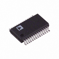
AD9220ARS Analog Devices Inc, AD9220ARS Datasheet - Page 14

AD9220ARS
Manufacturer Part Number
AD9220ARS
Description
A/D Converter (A-D) IC
Manufacturer
Analog Devices Inc
Specifications of AD9220ARS
Peak Reflow Compatible (260 C)
No
No. Of Bits
12 Bit
Leaded Process Compatible
No
Mounting Type
Surface Mount
No. Of Channels
2
Interface Type
Parallel
Package / Case
28-SSOP
Rohs Status
RoHS non-compliant
Number Of Bits
12
Sampling Rate (per Second)
10M
Data Interface
Parallel
Number Of Converters
7
Power Dissipation (max)
310mW
Voltage Supply Source
Single Supply
Operating Temperature
-40°C ~ 85°C
Number Of Elements
1
Resolution
12Bit
Architecture
Pipelined
Sample Rate
10MSPS
Input Polarity
Unipolar
Input Type
Voltage
Rated Input Volt
±1/±2.5V
Differential Input
Yes
Power Supply Requirement
Analog and Digital
Single Supply Voltage (typ)
5V
Single Supply Voltage (min)
4.75V
Single Supply Voltage (max)
5.25V
Dual Supply Voltage (typ)
Not RequiredV
Dual Supply Voltage (min)
Not RequiredV
Dual Supply Voltage (max)
Not RequiredV
Power Dissipation
310mW
Differential Linearity Error
±0.75LSB
Integral Nonlinearity Error
±1.25LSB
Operating Temp Range
-40C to 85C
Operating Temperature Classification
Industrial
Mounting
Surface Mount
Pin Count
28
Package Type
SSOP
Lead Free Status / RoHS Status
Contains lead / RoHS non-compliant
For Use With
AD9220-EB - BOARD EVAL FOR AD9220
Lead Free Status / Rohs Status
Not Compliant
Available stocks
Company
Part Number
Manufacturer
Quantity
Price
Company:
Part Number:
AD9220ARS
Manufacturer:
AD
Quantity:
5 510
Part Number:
AD9220ARS
Manufacturer:
ADI/亚德诺
Quantity:
20 000
Part Number:
AD9220ARSZ
Manufacturer:
ADI/亚德诺
Quantity:
20 000
Part Number:
AD9220ARSZ-REEL
Manufacturer:
ADI/亚德诺
Quantity:
20 000
Part Number:
AD9220ARSZRL
Manufacturer:
ADI/亚德诺
Quantity:
20 000
AD9221/AD9223/AD9220
Reference
Operating Mode
INTERNAL
INTERNAL
INTERNAL
EXTERNAL
(Nondynamic)
EXTERNAL
(Dynamic)
DRIVING THE ANALOG INPUTS
Introduction
The AD9221/AD9223/AD9220 has a highly flexible input
structure, allowing it to interface with single-ended or differen-
tial input interface circuitry. The applications shown in sections
Driving the Analog Inputs and Reference Configurations, along
with the information presented in Input and Reference Over-
view of this data sheet, give examples of both single-ended and
differential operation. Refer to Tables I and II for a list of the
different possible input and reference configurations and their
associated figures in the data sheet.
The optimum mode of operation, analog input range, and asso-
ciated interface circuitry will be determined by the particular
application’s performance requirements as well as power supply
options. For example, a dc coupled single-ended input would be
appropriate for most data acquisition and imaging applications.
Also, many communication applications that require a dc coupled
input for proper demodulation can take advantage of the excel-
lent single-ended distortion performance of the AD9221/AD9223/
AD9220. The input span should be configured such that the
system’s performance objectives and the headroom requirements
of the driving op amp are simultaneously met.
Alternatively, the differential mode of operation with a transformer
coupled input provides the best THD and SFDR performance
over a wide frequency range. This mode of operation should be
considered for the most demanding spectral based applications
that allow ac coupling (e.g., Direct IF to Digital Conversion).
Single-ended operation requires that VINA be ac- or dc-coupled
to the input signal source while VINB of the AD9221/AD9223/
AD9220 can be biased to the appropriate voltage corresponding
to a midscale code transition. Note that signal inversion may be
easily accomplished by transposing VINA and VINB. The rated
specifications for the AD9221/AD9223/AD9220 are character-
ized using single-ended circuitry with input spans of 5 V and
2 V as well as VINB = 2.5 V.
Differential operation requires that VINA and VINB be simulta-
neously driven with two equal signals that are in and out of
phase versions of the input signal. Differential operation of the
Input Span (VINA–VINB)
(V p-p)
2
5
2 ≤ SPAN ≤ 5 and
SPAN = 2 × VREF
2 ≤ SPAN ≤ 5
2 ≤ SPAN ≤ 5
Table II. Reference Configuration Summary
Required VREF (V)
1
2.5
1 ≤ VREF ≤ 2.5 and
VREF = (1 + R1/R2)
1 ≤ VREF ≤ 2.5
CAPT and CAPB
Externally Driven
–14–
AD9221/AD9223/AD9220 offers the following benefits: (1)
Signal swings are smaller and therefore linearity requirements
placed on the input signal source may be easier to achieve, (2)
Signal swings are smaller and therefore may allow the use of op
amps that may otherwise have been constrained by headroom
limitations, (3) Differential operation minimizes even-order
harmonic products, and (4) Differential operation offers noise
immunity based on the device’s common-mode rejection.
Figure 11 depicts the common-mode rejection of the three devices.
As is typical of most CMOS devices, exceeding the supply limits
will turn on internal parasitic diodes, resulting in transient cur-
rents within the device. Figure 12 shows a simple means of
clamping an ac- or dc-coupled single-ended input with the
addition of two series resistors and two diodes. An optional capaci-
tor is shown for ac-coupled applications. Note that a larger
series resistor could be used to limit the fault current through
D1 and D2 but should be evaluated since it can cause a degrada-
tion in overall performance. A similar clamping circuit could also
be used for each input if a differential input signal is being applied.
Figure 11. AD9221/AD9223/AD9220 Input CMR vs.
Input Frequency
20
30
40
50
60
70
80
90
0.1
Connect
SENSE
SENSE
R1
R2
SENSE
VREF
SENSE
EXT. REF.
EXT. REF.
VREF
AD9220
1
FREQUENCY– MHz
AD9223
To
VREF
REFCOM
VREF and SENSE
SENSE and REFCOM
AVDD
EXT. REF.
AVDD
REFCOM
CAPT
CAPB
10
AD9221
100
REV. E


