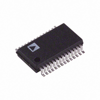
AD9220ARS Analog Devices Inc, AD9220ARS Datasheet - Page 21

AD9220ARS
Manufacturer Part Number
AD9220ARS
Description
A/D Converter (A-D) IC
Manufacturer
Analog Devices Inc
Specifications of AD9220ARS
Peak Reflow Compatible (260 C)
No
No. Of Bits
12 Bit
Leaded Process Compatible
No
Mounting Type
Surface Mount
No. Of Channels
2
Interface Type
Parallel
Package / Case
28-SSOP
Rohs Status
RoHS non-compliant
Number Of Bits
12
Sampling Rate (per Second)
10M
Data Interface
Parallel
Number Of Converters
7
Power Dissipation (max)
310mW
Voltage Supply Source
Single Supply
Operating Temperature
-40°C ~ 85°C
Number Of Elements
1
Resolution
12Bit
Architecture
Pipelined
Sample Rate
10MSPS
Input Polarity
Unipolar
Input Type
Voltage
Rated Input Volt
±1/±2.5V
Differential Input
Yes
Power Supply Requirement
Analog and Digital
Single Supply Voltage (typ)
5V
Single Supply Voltage (min)
4.75V
Single Supply Voltage (max)
5.25V
Dual Supply Voltage (typ)
Not RequiredV
Dual Supply Voltage (min)
Not RequiredV
Dual Supply Voltage (max)
Not RequiredV
Power Dissipation
310mW
Differential Linearity Error
±0.75LSB
Integral Nonlinearity Error
±1.25LSB
Operating Temp Range
-40C to 85C
Operating Temperature Classification
Industrial
Mounting
Surface Mount
Pin Count
28
Package Type
SSOP
Lead Free Status / RoHS Status
Contains lead / RoHS non-compliant
For Use With
AD9220-EB - BOARD EVAL FOR AD9220
Lead Free Status / Rohs Status
Not Compliant
Available stocks
Company
Part Number
Manufacturer
Quantity
Price
Company:
Part Number:
AD9220ARS
Manufacturer:
AD
Quantity:
5 510
Part Number:
AD9220ARS
Manufacturer:
ADI/亚德诺
Quantity:
20 000
Part Number:
AD9220ARSZ
Manufacturer:
ADI/亚德诺
Quantity:
20 000
Part Number:
AD9220ARSZ-REEL
Manufacturer:
ADI/亚德诺
Quantity:
20 000
Part Number:
AD9220ARSZRL
Manufacturer:
ADI/亚德诺
Quantity:
20 000
can be detected. Table V is a truth table for the over/underrange
circuit in Figure 28, which uses NAND gates. Systems requiring
programmable gain conditioning of the AD9221/AD9223/
AD9220 input signal can immediately detect an out-of-range
condition, thus eliminating gain selection iterations. Also, OTR
can be used for digital offset and gain calibration.
OTR
0
0
1
1
Digital Output Driver Considerations (DVDD)
The AD9221, AD9223 and AD9220 output drivers can be
configured to interface with 5 V or 3.3 V logic families by setting
DVDD to 5 V or 3.3 V respectively. The AD9221/AD9223/
AD9220 output drivers are sized to provide sufficient output
current to drive a wide variety of logic families. However, large
drive currents tend to cause glitches on the supplies and may
affect SINAD performance. Applications requiring the AD9221/
AD9223/AD9220 to drive large capacitive loads or large fanout
may require additional decoupling capacitors on DVDD. In
extreme cases, external buffers or latches may be required.
Clock Input and Considerations
The AD9221/AD9223/AD9220 internal timing uses the two
edges of the clock input to generate a variety of internal timing
signals. The clock input must meet or exceed the minimum
specified pulsewidth high and low (t
for the given A/D as defined in the Switching Specifications to
meet the rated performance specifications. For example, the
clock input to the AD9220 operating at 10 MSPS may have a
duty cycle between 45% to 55% to meet this timing requirement
since the minimum specified t
rates below 10 MSPS, the duty cycle may deviate from this
range to the extent that both t
All high speed high resolution A/Ds are sensitive to the quality
of the clock input. The degradation in SNR at a given full-scale
input frequency (f
calculated with the following equation:
REV. E
Figure 28. Overrange or Underrange Logic
MSB
OTR
MSB
Table V. Out-of-Range Truth Table
SNR
IN
) due to only aperture jitter (t
MSB
0
1
0
1
=
20
log
CH
CH
10
and t
and t
[
1 2
/ π
CH
CL
CL
and t
f
IN
is 45 ns. For clock
are satisfied.
Analog Input Is
In Range
In Range
Underrange
Overrange
t
CL
A
OVER = “1”
UNDER = “1”
]
) specifications
A
) can be
–21–
In the equation, the rms aperture jitter, t
sum square of all the jitter sources, which include the clock
input, analog input signal, and A/D aperture jitter specification.
For example, if a 5 MHz full-scale sine wave is sampled by an
A/D with a total rms jitter of 15 ps, the SNR performance of the
A/D will be limited to 66.5 dB. Undersampling applications are
particularly sensitive to jitter.
The clock input should be treated as an analog signal in cases
where aperture jitter may affect the dynamic range of the AD9221/
AD9223/AD9220. As such, supplies for clock drivers should be
separated from the A/D output driver supplies to avoid modulating
the clock signal with digital noise. Low jitter crystal controlled
oscillators make the best clock sources. If the clock is generated
from another type of source (by gating, dividing, or other method),
it should be retimed by the original clock at the last step.
Most of the power dissipated by the AD9221/AD9223/AD9220
is from the analog power supplies. However, lower clock speeds
will reduce digital current slightly. Figure 29 shows the relation-
ship between power and clock rate for each A/D.
Figure 29a. AD9221 Power Consumption vs. Clock
Frequency
Figure 29b. AD9223 Power Consumption vs. Clock
Frequency
125
120
115
110
105
100
66
64
62
60
58
56
54
52
50
48
95
90
0
0.5
1
AD9221/AD9223/AD9220
CLOCK FREQUENCY – MHz
CLOCK FREQUENCY – MHz
1.0
2
5V p-p
5V p-p
1.5
3
2V p-p
2V p-p
2.0
A
4
, represents the root-
2.5
5
3.0
6


