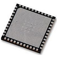
LTC3675EUFF#PBF Linear Technology, LTC3675EUFF#PBF Datasheet - Page 7

LTC3675EUFF#PBF
Manufacturer Part Number
LTC3675EUFF#PBF
Description
IC, PMIC, 1A, QFN-44
Manufacturer
Linear Technology
Datasheet
1.LTC3675EUFFPBF.pdf
(36 pages)
Specifications of LTC3675EUFF#PBF
Supply Voltage
5.5V
No. Of Step-down Dc - Dc Converters
4
No. Of Ldo Regulators
1
Digital Ic Case Style
QFN
No. Of Pins
44
No. Of Regulated Outputs
7
Operating Temperature Range
-40°C To +125°C
Rohs Compliant
Yes
Lead Free Status / RoHS Status
Lead free / RoHS Compliant
Available stocks
Company
Part Number
Manufacturer
Quantity
Price
ELECTRICAL CHARACTERISTICS
temperature range, otherwise specifi cations are at T
SYMBOL
t
t
t
t
t
t
t
t
t
t
t
t
Interface Logic Pins (PBSTAT, WAKE, RSTB, IRQB, ONB)
I
V
V
V
Interface Logic Pins (EN1, EN2, EN3, EN4, ENBB)
V
V
V
I
Pushbutton Parameters; CT = 0.01μF
t
t
t
t
t
t
Note 1: Stresses beyond those listed under Absolute Maximum Ratings
may cause permanent damage to the device. Exposure to any Absolute
Maximum Rating condition for extended periods may affect device
reliability and lifetime.
Note 2: The LTC3675 is guaranteed to meet performance specifi cations
from the 0°C to 125°C operating junction temperature range. Specifi cations
over the –40°C to 125°C operating junction temperature range are assured
by design, characterization and correlation with statistical process controls.
Note 3: The LTC3675 includes overtemperature protection which protects
the device during momentary overload conditions. Junction temperature
will exceed 125°C when overtemperature protection is active. Continuous
operation above the specifi ed maximum operating junction temperature
may impair device reliability.
BUF
HD_SDA
SU_STA
SU_STO
HD_DAT(O)
HD_DAT(I)
SU_DAT
LOW
HIGH
f
r
SP
LK(HIGH)
EN
ONB_LO
ONB_WAKE
ONB_HR
HR
PBSTAT_PW
WAKE_ON
OL
ONB(HIGH)
ONB(LOW)
HI_ALLOFF
EN_HYS
HI
PARAMETER
Bus Free Time Between Stop and Start
Condition
Hold Time After Repeated Start Condition
Repeated Start Condition Set-Up Time
Stop Condition Set-Up Time
Data Hold Time Output
Data Hold Time Input
Data Set-Up Time
SCL Clock Low Period
SCL Clock High Period
Clock/Data Fall Time
Clock/Data Rise Time
Input Spike Suppression Pulse Width
Output High Leakage Current
Output Low Voltage
ONB High Threshold
ONB Low Threshold
Enable Rising Threshold
Enable Falling Hysteresis
Enable Rising Threshold
Enable Pin Leakage Current
ONB Low Time to PBSTAT Low
ONB Low Time to WAKE High
ONB Low to Hard Reset
Time for Which All Enabled Regulators are
Disabled
PBSTAT Minimum Pulse Width
WAKE High Time
A
= 25°C. V
CONDITIONS
C
C
3.6V at Pin
3mA into Pin
All Regulators and LED Driver Disabled
At Least One Regulator/LED Driver Enabled
EN = 3.6V
WAKE High
B
B
= Capacitance of One Bus Line (pF)
= Capacitance of One Bus Line (pF)
The
l
IN
denotes the specifi cations which apply over the full operating
= 3.6V.
Note 4: Static current, switches not switching. Actual current may be
higher due to gate charge losses at the switching frequency.
Note 5: Currents measured at a specifi c V
Buck 2 (V
Boost (V
Note 6: The current limit features of this part are intended to protect the
IC from short term or intermittent fault conditions. Continuous operation
above the maximum specifi ed pin current rating may result in device
degradation over time.
Note 7: With dual string operation, the LED pin with the lower voltage sets
the regulation point.
IN
IN
, Pin 34); LED driver (V
, Pin 7); Buck 3 and Buck 4 (V
l
l
IN
20+0.1C
20+0.1C
, Pin 31).
MIN
100
400
400
380
280
1.3
0.6
0.6
0.6
1.3
0.6
3.5
0.7
3.5
–1
–1
28
28
0
0
IN
IN
B
B
, Pin 10); Boost and Buck
pin. Buck 1 (V
TYP
100
800
700
650
400
400
60
50
50
5
1
5
LTC3675
1200
1200
MAX
IN
900
300
300
400
420
520
6.5
1.3
6.5
50
72
72
1
1
, Pin 6);
UNITS
7
3675f
mV
mV
mV
mV
mV
mV
sec
sec
sec
ms
ms
ms
μA
μA
μs
μs
μs
μs
ns
ns
ns
μs
μs
ns
ns
ns


