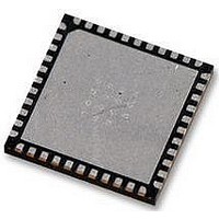
LTC3675EUFF#PBF Linear Technology, LTC3675EUFF#PBF Datasheet - Page 27

LTC3675EUFF#PBF
Manufacturer Part Number
LTC3675EUFF#PBF
Description
IC, PMIC, 1A, QFN-44
Manufacturer
Linear Technology
Datasheet
1.LTC3675EUFFPBF.pdf
(36 pages)
Specifications of LTC3675EUFF#PBF
Supply Voltage
5.5V
No. Of Step-down Dc - Dc Converters
4
No. Of Ldo Regulators
1
Digital Ic Case Style
QFN
No. Of Pins
44
No. Of Regulated Outputs
7
Operating Temperature Range
-40°C To +125°C
Rohs Compliant
Yes
Lead Free Status / RoHS Status
Lead free / RoHS Compliant
Available stocks
Company
Part Number
Manufacturer
Quantity
Price
APPLICATIONS INFORMATION
a 47μF capacitor for a 2A combined buck regulator and
22μF for a 1A combined buck regulator. Refer to “Capaci-
tor Selection” in the Applications Information section for
details on selecting a proper capacitor.
Boost Regulator
The boost regulator is designed to be used with a 2.2μH
inductor. Table 8 provides a list of recommended inductors.
Table 6. Buck Regulator Program Register Bit Format
Bit7
Bit6
Bit5
Bit4
Bit3(DAC3)
Bit2(DAC2)
Bit1(DAC1)
Bit0(DAC0)
Table 7. Recommended Inductors for 2A Combined Buck Regulator
PART NUMBER
XFL4022-222
LPS6225-222
FDV0530-2R2
Table 8. Recommended Inductors for Boost Regulator and Buck-Boost Regulator
PART NUMBER
XFL4022-222
LTF5022-2R2
Table 9. Boost Regulator Program Register Bit Format
Bit7
Bit6
Bit5
Bit4
Bit3(DAC3)
Bit2(DAC2)
Bit1(DAC1)
Bit0(DAC0)
Enable
OUT_Hi-Z
Mode
Slow Edge
DAC Control
Enable
x
Mode
Slow Edge
DAC Control
L(μH)
L(μH)
2.2
2.2
2.2
2.2
2.2
Default is '0' which disables the part. A buck regulator can also be enabled via its enable pin.
When enabled via pin, the contents of the I
Default is ‘1’ in which the SW node remains in a high impedance state when the regulator is in shutdown.
A ‘0’ pulls the SW node to GND through a 10k resistor.
Default is ‘1’ which is Burst Mode operation. A ‘0’ programs the regulator to operate in pulse-skipping mode.
This bit controls the slew rate of the switch node. Default is '0' which enables the switch node to slew at a
faster rate, than if the bit were programmed a '1'.
These bits are used to program the feedback regulation voltage. Default is '1111' which programs a full-scale
voltage of 800mV. Bits '0000' program the lowest feedback regulation of 425mV. A LSB (DAC0) has a bit
weight of 25mV.
MAX I
MAX I
3.5
5.3
3.5
3.2
4
DC
DC
(A)
(A)
Default is ‘0’ which disables the boost.
Unused
Mode = 0 is PWM mode, Mode = 1 is Burst Mode operation
This bit controls the slew rate of the switch node. Default is ‘0’ which enables the switch node
to slew at a faster rate than if the bit were programmed a ‘1.’
These bits are used to program the feedback regulation voltage. Default is ‘1111’ which
programs a full-scale voltage of 800mV. Bits ‘0000’ program the lowest feedback regulation of
425mV. A LSB (DAC0) has a bit weight of 25mV.
MAX DCR (mΩ)
MAX DCR (mΩ)
21.35
21.35
17.3
45
36
The input supply needs to be decoupled with a 10μF
capacitor while the output needs to be decoupled with
two 22μF capacitors. Refer to Capacitor Selection in the
Applications Information section for details on selecting
a proper capacitor.
The boost regulator can be programmed via I
gram the boost regulator, use sub-address 05h. The bit
format is explained in Table 9.
2
C register program its functionality.
SIZE IN mm (L × W × H)
SIZE IN mm (L × W × H)
6.2 × 5.8 × 3
5 × 5.2 × 2.2
6 × 6 × 2.5
4 × 4 × 2
4 × 4 × 2
MANUFACTURER
Coilcraft
www.coilcraft.com
Coilcraft
www.coilcraft.com
Toko
www.toko.com
MANUFACTURER
Coilcraft
www.coilcraft.com
TDK
www.tdk.com
LTC3675
2
C. To pro-
27
3675f


