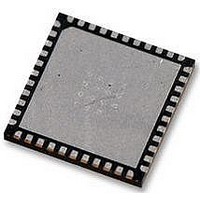
LTC3675EUFF#PBF Linear Technology, LTC3675EUFF#PBF Datasheet - Page 29

LTC3675EUFF#PBF
Manufacturer Part Number
LTC3675EUFF#PBF
Description
IC, PMIC, 1A, QFN-44
Manufacturer
Linear Technology
Datasheet
1.LTC3675EUFFPBF.pdf
(36 pages)
Specifications of LTC3675EUFF#PBF
Supply Voltage
5.5V
No. Of Step-down Dc - Dc Converters
4
No. Of Ldo Regulators
1
Digital Ic Case Style
QFN
No. Of Pins
44
No. Of Regulated Outputs
7
Operating Temperature Range
-40°C To +125°C
Rohs Compliant
Yes
Lead Free Status / RoHS Status
Lead free / RoHS Compliant
Available stocks
Company
Part Number
Manufacturer
Quantity
Price
APPLICATIONS INFORMATION
Table 13. LED Driver Regulator Program Register 1 Bit Format
Bit7
Bit6
Bit5
Bit4
Bit3
Bit2(GRAD2)
Bit1(GRAD1)
Bit0(GRAD0)
These times are shown in Table 14. The default state of
000 in GRAD[2:0] results in a very fast ramp time that
cannot be visually perceived.
Table 14. LED Gradation Bits
GRAD2, GRAD1, GRAD0
000
001
010
011
100
101
110
111 (Default)
The LED DAC register is at sub-address 08h. All 8 bits in
this register are used to control LED current. The default
state of this register is 00h which disables the LED driver.
See Table 1.
Operating the LED Driver As a High Voltage Boost
Regulator
The LED driver may be confi gured as a high voltage boost
regulator capable of producing an output voltage up to
40V. The boost mode may be programmed via I
this mode, the LED_OV pin serves as the feedback pin.
The feedback resistors are selected as discussed in the
Switching Regulator Output voltage and Feedback Network
section. The LED_FS pins must be tied to the input supply
in this mode. When confi gured as a high voltage boost,
the LED DAC register is ignored.
x
Mode1
Mode0
Slow Edge
2xFS
DAC Control
GRADATION STEP TIME
0.056 ms
0.912 ms
1.824 ms
3.648 ms
7.296 ms
14.592 ms
29.184 ms
58.368 ms
Unused
Mode1 = Mode0 = 0 is default; both LED pins are regulated.
Mode1 = 0 Mode0 = 1; Only LED1 is regulated. (Single string application).
Mode1 = 1 Mode0 = 0; LED driver is confi gured as a high voltage boost regulator.
Mode1 = Mode0 = 1; Both LED pins are regulated, but boost is not powered up. In this mode an external
voltage is needed to drive the LED’s.
This bit controls the slew rate of the switch node. Default is ‘0’ which enables the switch node to slew at a
faster rate than if the bit were programmed a ‘1.’
This bit doubles the full-scale programmed LED current. Default is ‘1.’
LED current gradation timing bits. Default is ‘111.’ See Table 14.
2
C. In
To maintain stability, the average inductor current must
be maintained below 750mA. This limits the deliverable
output current at low input supply voltages. Figure 8 gives
an example of the LED driver confi gured as a high voltage
boost regulator.
Input and Output Decoupling Capacitor Selection
The LTC3675 has multiple input supply pins and output
pins. Each of these pins must be decoupled with low ESR
capacitors to GND. These capacitors must be placed as
close to the pins as possible. Ceramic dielectric capacitors
are a good compromise between high dielectric constant
and stability versus temperature and DC bias. Note that the
capacitance of a capacitor deteriorates at higher DC bias.
It is important to consult manufacturer data sheets and
obtain the true capacitance of a capacitor at the DC bias
voltage it will be operated at. For this reason, avoid the
use of Y5V dielectric capacitors. The X5R/X7R dielectric
capacitors offer good overall performance.
The input supply voltage pins 6, 7, 10 and 40 all need
to be decoupled with at least 10μF capacitors. The input
supply pins 31 and 34 and the DVCC pin 41 need to be
decoupled with 2.2μF capacitors. The outputs of the 1A
buck regulators need 22μF capacitors, while the outputs
of the 500mA buck regulators need 10μF capacitors. The
buck-boost output regulator needs a 22μF decoupling
capacitor. The boost regulator needs two 22μF output
decoupling capacitors. The LED driver output pin should
be decoupled with a 4.7μF capacitor.
LTC3675
29
3675f


