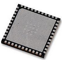
LTC3675EUFF#PBF Linear Technology, LTC3675EUFF#PBF Datasheet - Page 15

LTC3675EUFF#PBF
Manufacturer Part Number
LTC3675EUFF#PBF
Description
IC, PMIC, 1A, QFN-44
Manufacturer
Linear Technology
Datasheet
1.LTC3675EUFFPBF.pdf
(36 pages)
Specifications of LTC3675EUFF#PBF
Supply Voltage
5.5V
No. Of Step-down Dc - Dc Converters
4
No. Of Ldo Regulators
1
Digital Ic Case Style
QFN
No. Of Pins
44
No. Of Regulated Outputs
7
Operating Temperature Range
-40°C To +125°C
Rohs Compliant
Yes
Lead Free Status / RoHS Status
Lead free / RoHS Compliant
Available stocks
Company
Part Number
Manufacturer
Quantity
Price
PIN FUNCTIONS
PBSTAT (Pin 25): Pushbutton Status Pin. Open drain
output. This pin provides a debounced and glitch free
status of the ONB pin.
WAKE (Pin 26): Open Drain Output. When the ONB pin
is pressed and released, the signal is debounced and the
WAKE signal is held HIGH for a minimum time period that
is scaled by the C
LED_FS (Pin 27): A resistor connected from this pin to
GND programs full-scale LED current.
ONB (Pin 28): Pushbutton Input. Active low.
LDOFB (Pin 29): LDO Feedback Pin. A resistor divider
from LDO_OUT to GND provides feedback.
LDO_OUT (Pin 30): Output of Always-On LDO. Decouple
with a 10μF capacitor to GND.
V
Switching Control Circuitry. A 2.2μF decoupling capacitor
to GND is recommended. Must be connected to all other
V
SW5 (Pin 32): Boost Regulator Switch Node. External
inductor connects to this pin.
V
22μF capacitors to GND.
V
Switching Control Circuitry. A 2.2μF decoupling capacitor
to GND is recommended. Must be connected to all other
V
IN
IN
OUT5
IN
IN
supply pins (Pins 6, 7, 10, 34, 40).
supply pins (Pins 6, 7, 10, 31, 40).
(Pin 31): Quiet Input Supply Used to Power Non-
(Pin 34): Quiet Input Supply Used to Power Non-
(Pin 33): Boost Regulator Output. Connect two
T
capacitor.
FB5 (Pin 35): Boost Regulator Feedback Pin. Receives feed-
back by a resistor divider connected across the output.
FB6 (Pin 36): Buck-Boost Regulator Feedback Pin. Re-
ceives feedback by a resistor divider connected across
the output.
ENBB (Pin 37): Buck-Boost Regulator Enable Input. Ac-
tive high.
SWAB6 (Pin 38): Buck-Boost Regulator Switch Pin. Ex-
ternal inductor connects to this pin and SWCD6.
SCL (Pin 39): Clock Line for I
V
decoupling capacitor to GND is recommended. Must be
connected to all other V
34).
DV
V
a 22μF capacitor to GND.
SDA (Pin 43): Serial Data Line for I
output during readback.
SWCD6 (Pin 44): Buck-Boost Regulator Switch Pin. Ex-
ternal inductor connects to this pin and SWAB6.
GND (Exposed Pad Pin 45): Ground for Entire Chip. Must
be soldered to PCB for electrical contact and rated thermal
performance.
IN
OUT6
CC
(Pin 40): Buck-Boost Regulator Input Supply. A 10μF
(Pin 41): Supply Pin for I
(Pins 42): Buck-Boost Regulator Output. Connect
IN
supply pins (Pins 6, 7, 10, 31,
2
C Port.
2
C Port.
2
C Port. Open drain
LTC3675
15
3675f


