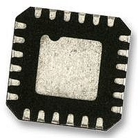
ADP5587ACPZ-R7 Analog Devices Inc, ADP5587ACPZ-R7 Datasheet - Page 8

ADP5587ACPZ-R7
Manufacturer Part Number
ADP5587ACPZ-R7
Description
IC, I/O EXPANDER, 400KHZ, LFCSP-24
Manufacturer
Analog Devices Inc
Type
I²C Port Expanderr
Datasheet
1.ADP5587ACPZ-R7.pdf
(24 pages)
Specifications of ADP5587ACPZ-R7
Bus Frequency
400kHz
Ic Interface Type
I2C
No. Of I/o's
18
Supply Voltage Range
1.7V To 3.6V
Digital Ic Case Style
LFCSP
No. Of Pins
24
Msl
MSL 3 - 168 Hours
Supply Voltage Max
3.6V
Applications
Cell Phone
Mounting Type
Surface Mount
Package / Case
24-LFCSP
Interface Type
I2C
Lead Free Status / RoHS Status
Lead free / RoHS Compliant
Other names
ADP5587ACPZ-R7TR
ADP5587
THEORY OF OPERATION
The ADP5587 is a GPIO expander that can be configured either
as an 18 I/O port expander or as a 10 column × 8 row keypad
matrix (80 keys maximum). It is ideal for cellular phone designs
and other portable devices that require a large extended keypad
and/or expanded I/Os. When smaller size keypads are required,
unused GPIOs in the keypad matrix can be used as I/Os (GPOs
and GPIs). All GPIOs (rows and columns) default to GPIs at
power-up with pull-ups and debounce enabled.
KEYPAD OPERATION
Any number of rows and columns, up to 10 columns × 8 rows,
can be configured to be part of the keypad matrix. The rows and
columns that make up the keypad matrix must be configured by
setting the corresponding bits in Register 0x1D to Register 0x1F.
Key presses and releases appear in the key event table/registers
with a decimal value of 1 (0x01 hexadecimal or 0000001 binary)
through a decimal value of 80 (0x50 hexadecimal or 1010000
binary). See Table 9 for key event number assignments. The
keypad, in idle mode, is configured with columns driven low
and rows as inputs configured high with pull-up resistors.
V
CC
SCL
SDA
RST
INT
GND
SDA
SCL
RST
V
INT
CC
19
21
23
22
20
24
G7
A7
B7
C7
D7
E7
F7
H7
J7
I7
1
A6
B6
C6
D6
G6
H6
E6
F6
J6
I6
2
REGISTERS
CONTROL
A5
B5
C5
D5
E5
G5
H5
F5
J5
I5
3
G4
A4
B4
C4
D4
E4
F4
H4
J4
I4
Figure 9. Typical Operating Circuit
4
A3
B3
C3
D3
G3
H3
E3
F3
J3
I3
5
Rev. B | Page 8 of 24
A2
B2
C2
D2
G2
H2
E2
F2
J2
I2
6
A1
B1
C1
D1
E1
G1
H1
F1
J1
I1
7
A0
B0
C0
D0
E0
G0
H0
F0
J0
I0
8
9
INTERFACE
Table 9. Key Event Number Assignment Table
Row
R0
R1
R2
R3
R4
R5
R6
R7
When one key press or multiple key presses (short between
column and row) occur, the internal state machine checks the
row pins to determine which one is driven low and then triggers
an internal interrupt. The state machine then starts a key scan
cycle to determine which columns are involved in the key press.
After a key has been pressed for 25 ms, the state machine sets
the appropriate key number in the key event status register with
the key-pressed bits set (the MSB in the key event register) in
the order detected. The state machine then sets the KE_INT bit
in Register 0x02. If the KE_IEN field in Register 0x01 is set, an
interrupt is sent to the host processor.
CONTROL
10
11
12
C0
1
11
21
31
41
51
61
71
13
C1
2
12
22
32
42
52
62
72
14
ADP5587
15
C2
3
13
23
33
43
53
63
73
16
18
17
C3
4
14
24
34
44
54
64
74
C9
C8
C4
5
15
25
35
45
55
65
75
C5
6
16
26
36
46
56
66
76
C6
7
17
27
37
47
57
67
77
C7
8
18
28
38
48
58
68
78
C8
9
19
29
39
49
59
69
79
C9
10
20
30
40
50
60
70
80


