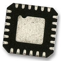
ADP5587ACPZ-R7 Analog Devices Inc, ADP5587ACPZ-R7 Datasheet - Page 13

ADP5587ACPZ-R7
Manufacturer Part Number
ADP5587ACPZ-R7
Description
IC, I/O EXPANDER, 400KHZ, LFCSP-24
Manufacturer
Analog Devices Inc
Type
I²C Port Expanderr
Datasheet
1.ADP5587ACPZ-R7.pdf
(24 pages)
Specifications of ADP5587ACPZ-R7
Bus Frequency
400kHz
Ic Interface Type
I2C
No. Of I/o's
18
Supply Voltage Range
1.7V To 3.6V
Digital Ic Case Style
LFCSP
No. Of Pins
24
Msl
MSL 3 - 168 Hours
Supply Voltage Max
3.6V
Applications
Cell Phone
Mounting Type
Surface Mount
Package / Case
24-LFCSP
Interface Type
I2C
Lead Free Status / RoHS Status
Lead free / RoHS Compliant
Other names
ADP5587ACPZ-R7TR
275 Microsecond Interrupt Configuration
The ADP5587 gives the user the flexibility of deasserting the
interrupt for 275 μs while there is a pending event. When the
INT_CFG bit in Register 0x01 is set, any attempt to clear the
interrupt bit while the interrupt pin is already asserted results
in a 275 μs deassertion. When the INT_CFG bit is cleared, the
processor interrupt remains asserted if the host tries to clear
the interrupt. This feature is particularly useful for software
development and edge triggering applications.
Debouncing
The ADP5587 has a 275 μs debounce time for GPIOs configured
as GPIs and rows in keypad scanning mode. The reset line
always has a 275 μs debounce time.
Table 14. Device Configuration
Matrix
10 × 8
8 × 8
8 × 7
8 × 6
8 × 5
7 × 7
7 × 6
7 × 5
6 × 6
6 × 5
6 × 4
…
0 × 0
Active Pins
C0 to C9, R0 to R7
C0 to C7, R0 to R7
C0 to C7, R0 to R6
C0 to C7, R0 to R5
C0 to C7, R0 to R4
C0 to C6, R0 to R6
C0 to C6, R0 to R5
C0 to C6, R0 to R4
C0 to C5, R0 to R5
C0 to C5, R0 to R4
C0 to C5, R0 to R3
…
None
Keypad
Number of Keys
80
64
56
48
40
49
42
35
36
30
24
…
0
Rev. B | Page 13 of 24
Available GPIO
0
C8, C9
R7, C8, C9
R6, R7, C8, C9
R5 to R7, C8, C9
R7, C7 to C9
R6, R7, C7 to C9
R5 to R7, C7 to C9
R6, R7, C6 to C9
R5 to R7, C6 to C9
R4 to R7, C6 to C9
…
R0 to R7, C0 to C9
General-Purpose Outputs (GPOs)
The ADP5587 allows the user to configure all or some of its
GPIOs as GPOs. These GPOs can be used as extra enables for
the host processor or simply as trigger outputs. When configured
as an output (GPO), a digital buffer drives the pin to 0 V for a 0
and to V
the corresponding bits in Register 0x1D through Register 0x1F are
set for GPIO mode; then use Register 0x23 through Register 0x25
to set the corresponding bits for GPO mode.
Power-On Reset
For built-in power-up initialization for applications lacking a
power-on reset signal, a reset pin, RST , allows the user to reset
the registers to default values in the event of a brownout or
other reset condition.
CC
for a 1. To set any GPIO as a GPO, make sure that
GPIO
Number of GPIOs
0
2
3
4
5
4
5
6
6
7
8
…
18
ADP5587


