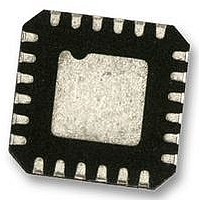
ADP5587ACPZ-R7 Analog Devices Inc, ADP5587ACPZ-R7 Datasheet - Page 6

ADP5587ACPZ-R7
Manufacturer Part Number
ADP5587ACPZ-R7
Description
IC, I/O EXPANDER, 400KHZ, LFCSP-24
Manufacturer
Analog Devices Inc
Type
I²C Port Expanderr
Datasheet
1.ADP5587ACPZ-R7.pdf
(24 pages)
Specifications of ADP5587ACPZ-R7
Bus Frequency
400kHz
Ic Interface Type
I2C
No. Of I/o's
18
Supply Voltage Range
1.7V To 3.6V
Digital Ic Case Style
LFCSP
No. Of Pins
24
Msl
MSL 3 - 168 Hours
Supply Voltage Max
3.6V
Applications
Cell Phone
Mounting Type
Surface Mount
Package / Case
24-LFCSP
Interface Type
I2C
Lead Free Status / RoHS Status
Lead free / RoHS Compliant
Other names
ADP5587ACPZ-R7TR
ADP5587
PIN CONFIGURATIONS AND FUNCTION DESCRIPTIONS
Table 8. Pin Function Descriptions
LFCSP
Pin No.
1
2
3
4
5
6
N/A
7
8
9
10
11
12
13
14
15
16
17
18
19
20
21
22
23
24
EP
WLCSP
Pin No.
A5
B5
C5
D5
E5
A4
B4
C4
D4
E4
A3
B3
C3
D3
E3
A2
B2
C2
D2
E2
A1
B1
C1
D1
E1
N/A
Figure 3. LFCSP Pin Configuration
(Not to Scale)
ADP5587
Mnemonic
R7
R6
R5
R4
R3
R2
N/A
R1
R0
C0
C1
C2
C3
C4
C5
C6
C7
C8
C9
GND
RST
V
SDA
SCL
INT
EPAD
TOP VIEW
CC
Description
GPIO, Row 7 in the Keypad Matrix.
GPIO, Row 6 in the Keypad Matrix.
GPIO, Row 5 in the Keypad Matrix.
GPIO, Row 4 in the Keypad Matrix.
GPIO, Row 3 in the Keypad Matrix.
GPIO, Row 2 in the Keypad Matrix.
No Connect (NC)
GPIO, Row 1 in the Keypad Matrix.
GPIO, Row 0 in the Keypad Matrix.
GPIO, Column 0 in the Keypad Matrix.
GPIO, Column 1 in the Keypad Matrix.
GPIO, Column 2 in the Keypad Matrix.
GPIO, Column 3 in the Keypad Matrix.
GPIO, Column 4 in the Keypad Matrix.
GPIO, Column 5 in the Keypad Matrix.
GPIO, Column 6 in the Keypad Matrix.
GPIO, Column 7 in the Keypad Matrix.
GPIO, Column 8 in the Keypad Matrix.
GPIO, Column 9 in the Keypad Matrix.
Ground.
Hardware Reset (Active Low). This pin resets the device to the power default conditions. The reset
pin must be driven low for a minimum of 50 μs to be valid and to prevent false resets due to ESD
glitches or noise in the system. If not used, RST must be tied high with a pull-up resistor.
Supply Voltage, 1.65 V to 3.6 V.
I
I
Processor Interrupt, Active Low, Open Drain. This pin can be pulled up to 2.7 V or 1.8 V for selection
flexibility in the processor GPIO supply group.
Exposed Pad. The exposed pad must be connected to ground.
2
2
C Serial Data. The open drain requires an external pull-up resistor.
C Clock.
Rev. B | Page 6 of 24
A
D
E
NOTES
1. NC = NO CONNECT.
B
C
Figure 4. WLCSP Pin Configuration
BALL A1
CORNER
RST
VCC
SDA
SCL
INT
1
(BALL SIDE DOWN)
GND
C6
C7
C8
C9
2
Not to Scale
TOP VIEW
C1
C2
C3
C4
C5
3
NC
R2
R1
R0
C0
4
R7
R6
R5
R4
R3
5


