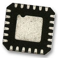
ADP5587ACPZ-R7 Analog Devices Inc, ADP5587ACPZ-R7 Datasheet

ADP5587ACPZ-R7
Specifications of ADP5587ACPZ-R7
Related parts for ADP5587ACPZ-R7
ADP5587ACPZ-R7 Summary of contents
Page 1
FEATURES 18-GPIO port expander or 10 × 8 keypad matrix GPIOs configurable as GPIs, GPOs, and keypad rows or columns interface with auto-increment 1. 3.6 V operation Keypad lock capability Open-drain interrupt output Key press ...
Page 2
ADP5587 TABLE OF CONTENTS Features .............................................................................................. 1 Applications ....................................................................................... 1 Functional Block Diagram .............................................................. 1 General Description ......................................................................... 1 Revision History ............................................................................... 2 Specifications ..................................................................................... 3 DC Characteristics ....................................................................... 3 AC Characteristics ........................................................................ 4 Absolute Maximum Ratings ............................................................ 5 Thermal ...
Page 3
SPECIFICATIONS −40°C to +85°C, unless otherwise noted CHARACTERISTICS Table 1. General DC Electrical Characteristics Parameter SUPPLY VOLTAGE V Input Voltage Range CC Supply Current 1 With One Key Press With GPI Low (Pull-Up ...
Page 4
ADP5587 AC CHARACTERISTICS Table 4. General AC Characteristics 1 Parameter Delay from Reset Deassertion Access Keypad Unlock Timer Keypad Interrupt Mask Timer Debounce 1 Guaranteed by design. Table Electrical Characteristics 2 Parameter ...
Page 5
ABSOLUTE MAXIMUM RATINGS Table 6. Parameter R7 SCL SDA RST INT GND Operating Ambient Temperature Range Operating Junction Temperature Range Storage Temperature Range ESD Machine Model ESD Human Body Model ESD Charged Device ...
Page 6
ADP5587 PIN CONFIGURATIONS AND FUNCTION DESCRIPTIONS ADP5587 TOP VIEW (Not to Scale) Figure 3. LFCSP Pin Configuration Table 8. Pin Function Descriptions LFCSP WLCSP Pin No. Pin No. Mnemonic ...
Page 7
TYPICAL PERFORMANCE CHARACTERISTICS T = 25°C, unless otherwise specified. A 3.5 3.0 2 3.0V CC 2.0 1.5 1.0 0.5 0 –40 – TEMPERATURE (°C) Figure 5. Standby (I ) Current vs. Temperature CC 140 120 ...
Page 8
ADP5587 THEORY OF OPERATION GND V CC SDA SCL SDA RST INT The ADP5587 is a GPIO expander that can be configured either I/O port expander column × 8 row keypad matrix (80 ...
Page 9
To prevent glitches or narrow press times registering as valid key presses, the key scanner requires the key to be pressed for two scan cycles. The key scanner has a sampling period of 25 ms; therefore, the key must be ...
Page 10
ADP5587 Auto-Increment The ADP5587 features automatic increment during I access, which allows the user to increment the address pointer without the need to send a read command for subsequent addresses. This minimizes processor intervention and, therefore, saves processor bandwidth and ...
Page 11
Keypad Lock/Unlock Feature The ADP5587 has a locking feature that allows the user to lock the keypad or GPIs (configured to be part of the event table). When enabled, the keypad lock can prevent generation of key event interrupts and ...
Page 12
ADP5587 GENERAL-PURPOSE INPUTS AND OUTPUTS The ADP5587 supports programmable GPIOs that can be configured to address a variety of uses. Figure 14 shows the makeup of a typical GPIO block where GPIOx represents any of the 18 ...
Page 13
Microsecond Interrupt Configuration The ADP5587 gives the user the flexibility of deasserting the interrupt for 275 μs while there is a pending event. When the INT_CFG bit in Register 0x01 is set, any attempt to clear the interrupt bit ...
Page 14
ADP5587 I C PROGRAMMING AND DIGITAL CONTROL 2 The ADP5587 provides full software programmability to facilitate its adoption in various product architectures. All register programming is done via the I 2 (01101001) for a read and Address 0x68 (01101000) for ...
Page 15
REGISTERS The general behavior of registers is as follows: • All registers are 0 on reset. • All registers are read/write unless otherwise specified. • Unused bits are read as 0. Table 15. Address Register Name 0x00 DEV_ID 0x01 CFG ...
Page 16
ADP5587 Address Register Name 0x2A DEBOUNCE_DIS2 0x2B DEBOUNCE_DIS3 0x2C GPIO_PULL1 0x2D GPIO_PULL2 0x2E GPIO_PULL3 REGISTER DESCRIPTIONS Table 16. DEV_ID—Register 0x00 (Device ID) Register Name Register Description DEV_ID Device ID[3:0], MFG ID[7:4] Table 17. CFG—Register 0x01 (Configuration Register 1) Field Bits ...
Page 17
Table 18. INT_STAT—Register 0x02 (Interrupt Status Register) Field Bits Not Used [7:4] OVR_FLOW_INT 1 3 K_LCK_INT 2 2 GPI_INT KE_INT The KE_INT, GPI_INT, and OVR_FLOW_INT bits reflect the status of the interrupts when ...
Page 18
ADP5587 Table 21. KP_LCK_TMR—Register 0x0E (Keypad Unlock 1 Timer to Keypad Unlock 2 Timer) Register Name Register Description KP_LCK_TMR Keypad Unlock 1 timer to Keypad Unlock 2 timer[2:0] (0: disabled, 1 sec to 7 sec) Keypad Lock Interrupt Mask Timer[7:3] ...
Page 19
Table 27. GPIO_INT_ENx—Register 0x1A to Register 0x1C (GPIO Interrupt Enable) Register Name Register Description GPIO_INT_EN1 GPIO interrupt enable (enables interrupts for (Register 0x1A) GP inputs only) GPIO_INT_EN2 GPIO interrupt enable (enables interrupts for (Register 0x1B) GP inputs only) GPIO_INT_EN3 GPIO ...
Page 20
ADP5587 Table 32. DEBOUNCE_DISx—Register 0x29 to Register 0x2B (Debounce Disable) Register Name Register Description DEBOUNCE_DIS1 Debounce disable (inputs) 0: enabled (Register 0x29) 1: disabled DEBOUNCE_DIS2 Debounce disable (inputs) (Register 0x2A) 0: enabled 1: disabled DEBOUNCE_DIS3 Debounce disable (inputs) (Register 0x2B) ...
Page 21
APPLICATIONS INFORMATION GND SCL SDA RST INT SCL SDA RST HOST PROCESSOR INT V CC GPI1 V CC GPI2 PWM OUTPUT APPLICATIONS OVERVIEW The ADP5587 is designed to complement host processors in a variety of ways. ...
Page 22
ADP5587 HOST PROCESSOR PWM KEYPAD MATRIX ...
Page 23
... SEATING PLANE 2.010 1.970 SQ 1.930 BALL A1 IDENTIFIER TOP VIEW (BALL SIDE DOWN) ORDERING GUIDE Model 1 Temperature Range ADP5587ACPZ-R7 −40°C to +85°C ADP5587ACBZ-R7 −40°C to +85° RoHS Compliant Part. 4.10 0.30 4.00 SQ 0.25 3.90 0.20 19 0.50 18 BSC ...
Page 24
ADP5587 NOTES I C refers to a communications protocol originally developed by Philips Semiconductors (now NXP Semiconductors). 2 ©2009-2010 Analog Devices, Inc. All rights reserved. Trademarks and registered trademarks are the property of their respective owners. D08612-0-5/10(B) Rev ...


