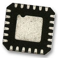
ADP5587ACPZ-R7 Analog Devices Inc, ADP5587ACPZ-R7 Datasheet - Page 14

ADP5587ACPZ-R7
Manufacturer Part Number
ADP5587ACPZ-R7
Description
IC, I/O EXPANDER, 400KHZ, LFCSP-24
Manufacturer
Analog Devices Inc
Type
I²C Port Expanderr
Datasheet
1.ADP5587ACPZ-R7.pdf
(24 pages)
Specifications of ADP5587ACPZ-R7
Bus Frequency
400kHz
Ic Interface Type
I2C
No. Of I/o's
18
Supply Voltage Range
1.7V To 3.6V
Digital Ic Case Style
LFCSP
No. Of Pins
24
Msl
MSL 3 - 168 Hours
Supply Voltage Max
3.6V
Applications
Cell Phone
Mounting Type
Surface Mount
Package / Case
24-LFCSP
Interface Type
I2C
Lead Free Status / RoHS Status
Lead free / RoHS Compliant
Other names
ADP5587ACPZ-R7TR
ADP5587
I
The ADP5587 provides full software programmability to
facilitate its adoption in various product architectures. All
register programming is done via the I
(01101001) for a read and Address 0x68 (01101000) for a write.
All communication to the ADP5587 is performed via its I
compatible serial interface. Figure 16 shows a typical write
sequence for programming an internal register. The cycle
begins with a start condition followed by the chip write address
(0x68). The ADP5587 acknowledges the chip write address byte
by pulling the data line low. The address of the register to which
data is to be written is sent next. The ADP5587 acknowledges
the register address byte by pulling the data line low. The data
byte to be written is sent next. The ADP5587 acknowledges the
data byte by pulling the data line low, and a stop condition
completes the sequence.
2
C PROGRAMMING AND DIGITAL CONTROL
ST 0
1
CHIP ADDRESS
1
0
ST 0
1
0
1
0 = WRITE
0
CHIP ADDRESS
1
0
0
0
ST 0
1
0
0
0
READ START ADDR
0 = WRITE
1
0
2
0
C bus at Address 0x69
CHIP ADDRESS
1
0
0
0
0
0
1
0
0
0
0
1
0 = WRITE
SUBADDRESS
0
0
1
Figure 17. I
0
0
0 ST 0
Figure 18. I
0
0
Figure 16. I
2
0
C-
Rev. B | Page 14 of 24
1
1
2
C Read and Write Sequences
SUBADDRESS
CHIP ADDRESS
1
1
2
C Read Auto-Increment
0 ST 0
0
2
C Write Sequence
1
0
1 = READ
0
1
Figure 17 shows a typical read sequence for reading back an
internal register. The cycle begins with a start condition
followed by the chip write address (0x68). The ADP5587
acknowledges the chip write address byte by pulling the data
line low. The address of the register from which data is to be
read is sent next. The ADP5587 acknowledges the register
address byte by pulling the data line low. The cycle continues
with a repeat start followed by the chip read address (0x69). The
ADP5587 acknowledges the chip read address byte by pulling
the data line low. The ADP5587 places the contents of the
previously addressed register on the bus for readback. There is
no acknowledge following the readback data byte, and a stop
condition completes the cycle.
CHIP ADDRESS
1
1
0
0
0
1
ADP5587 RECEIVES DATA
ADP5587 SENDS DATA 1
0
1 = READ
0
1
0
ADP5587 SENDS DATA
0
0 SP
...
ADP5587 SENDS DATA N
1 SP
1
ST


