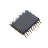
MAX1441GUP/V+ Maxim Integrated Products, MAX1441GUP/V+ Datasheet - Page 26

MAX1441GUP/V+
Manufacturer Part Number
MAX1441GUP/V+
Description
Touch Screen Converters & Controllers PROXIMITY SENSR el Proximity and Tou
Manufacturer
Maxim Integrated Products
Datasheet
1.MAX1441GUPV.pdf
(41 pages)
Specifications of MAX1441GUP/V+
Lead Free Status / RoHS Status
Lead free / RoHS Compliant
Automotive, Two-Channel Proximity and
Touch Sensor
Table 11. Special-Function Register Bit Description (continued)
26
ICDF[7:2]
ICDB (1Ch, 00h)
Initialization
Read/Write Access
ICDB[7:0]
ICDA (1Dh, 00h)
Initialization
Read/Write Access
ICDA[15:0]
ICDD (1Eh, 00h)
Initialization
Read/Write Access
ICDD[15:0]
AFEINTST (00h, 01h)
Initialization
Read/Write Access
AFEINTST.0–IDR1
AFEINTST.1–IDR2
AFEINTST.2–IWUP1
AFEINTST.3–IWUP2
AFEINTST[7:4]
REGISTER
Reserved. Read returns 0.
In-Circuit Debug Buffer Register (8-Bit Register)
This register is cleared to 00h after a power-on reset or a Test-Logic-Reset TAP state.
Unrestricted read/write by CPU.
In-Circuit Debug Buffer Bits [7:0]. ICDB serves as the parallel holding buffer for the debug shift
register of the TAP. Data is read from or written to ICDB for serial communication between the debug
function and the external host. This register is mapped to the SFR space for read/write access by the
CPU.
In-Circuit Debug Address Register (16-Bit Register)
This register is cleared to FFFFh after a power-on reset or a Test-Logic-Reset TAP state.
Unrestricted read by the CPU. This register can be accessed using a valid JTAG debug engine command.
In-Circuit Debug Address Bits [15:0]. This register serves as the address register for the debug engine
to store a specific location for the ROM code execution. This register is also used by the debug engine
as a mask register to mask out don’t care bits in the ICDD register when BP5 is used as a register
breakpoint. When a bit in this register is set to 1, the corresponding bit location in the ICDD register is
compared to the updating destination data to determine if a break should be generated. When a bit
in this register is cleared, the corresponding bit in the ICDD register becomes a don’t care and is not
compared against the updating data. When all bits in this register are cleared, any updated data pattern
causes a break when the BP5 register matches the destination register address of the current
instruction.
In-Circuit Debug Data Register (16-Bit Register)
This register is cleared to 0000h after a power-on reset or a Test-Logic-Reset TAP state.
Unrestricted read by the CPU. This register can be accessed using a valid JTAG debug engine command.
In-Circuit Debug Data Bits [15:0]. This register serves as the data/count register for the debug engine
to store data or read count for ROM code execution. This register is also used by the debug engine as a
data register for content matching when BP5 is used as a register breakpoint. In this case, only data bits
in this register with their corresponding mask bits in the ICDA register set is compared with the updated
destination data to determine if a break should be generated.
AFE Interrupt Status Register (8-Bit Register)
This register is cleared to 00h on all forms of reset.
Unrestricted read/write. See the following individual bit definitions for write restriction.
CH1 Data Ready Interrupt Flag. This bit is set to 1 when a new conversion result is available. This bit
remains set unless cleared by software.
CH2 Data Ready Interrupt Flag. This bit is set to 1 when a new conversion result is available. This bit
remains set unless cleared by software.
CH1 Wake-Up Event Interrupt Flag. This bit is set to 1 when a wake-up condition is detected. This bit
remains set unless cleared by software.
CH2 Wake-Up Event Interrupt Flag. This bit is set to 1 when a wake-up condition is detected. This bit
remains set unless cleared by software.
Reserved. Read returns 0.
DESCRIPTION


