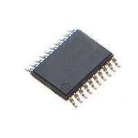
MAX1441GUP/V+ Maxim Integrated Products, MAX1441GUP/V+ Datasheet - Page 25

MAX1441GUP/V+
Manufacturer Part Number
MAX1441GUP/V+
Description
Touch Screen Converters & Controllers PROXIMITY SENSR el Proximity and Tou
Manufacturer
Maxim Integrated Products
Datasheet
1.MAX1441GUPV.pdf
(41 pages)
Specifications of MAX1441GUP/V+
Lead Free Status / RoHS Status
Lead free / RoHS Compliant
Table 11. Special-Function Register Bit Description (continued)
ICDC (1Ah, 00h)
Initialization
Read/Write Access
ICDC[3:0]–CMD[3:0]
ICDC.4
ICDC.5–REGE
ICDC.6–TE
ICDC.7–DME
ICDF (1Bh, 00h)
Initialization
Read/Write Access
ICDF.0–TXC
ICDF.1–SPE
REGISTER
Automotive, Two-Channel Proximity and
In-Circuit Debug Control Register (8-Bit Register)
This register is cleared to 00h after a power-on reset or a Test-Logic-Reset TAP state.
Unrestricted read; all bits are set and cleared by the debug engine only. This register can be accessed
using a valid JTAG debug engine command.
Command Bits [3:0]. These bits reflect the current host command in debug mode. These bits are set
by the debug engine and allow the ROM code to determine the course of action.
Reserved. Read returns 0.
Break-On Register Enable.
This bit always returns 0. Therefore, BP4 and BP5 breakpoints are not supported.
Timer Enabled.
This bit always returns 0 and the timer is automatically disabled in debug mode.
Debug Mode Enable. When this bit is cleared to 0, background mode commands can be executed but
breakpoints are disabled. When this bit is set to 1, breakpoints are enabled while background mode
commands can still be entered. This bit is only set or cleared from background mode. This bit has no
meaning for the ROM code.
In-Circuit Debug Flag Register (8-Bit Register)
This register is cleared to 00h after a power-on reset or a Test-Logic-Reset TAP state.
Unrestricted read; only bit 0 is writable by the CPU.
Serial Transfer Complete. This bit is set by the hardware at the end of a transfer cycle at the TAP
communication link. The TXC helps the debug engine to recognize host requests, either command or
data. This bit is normally set by ROM code to signify/request sending or receiving data; the TXC must
be cleared by the debug engine once set. CPU writes to the TXC bit result in clearing the JTAG PSS1:0
bits.
System Program Enable. The SPE bit used for in-system programming support and its logical state,
when read by the CPU, always reflects the logical-OR of the SPE bit and the SPE bit of the System
Programming Buffer (SPB) register in the TAP module (which is accessible using JTAG). The logical
state of this bit determines the program flow after a reset. When it is set to logic 1, in-system program-
ming is executed by the utility ROM. When it is cleared to 0, execution is transferred to user code. This
bit allows read access by the CPU and is cleared to 0 only on a power-on reset or Test-Logic-Reset. The
JTAG SPE bit is cleared by hardware when the ROD bit is set.
The SPE bit is read only.
CMD[3:0]
Other
0000
0001
0010
0011
0100
0101
0110
0111
1000
1001
1010
No operation
Read register
Read data memory
Read stack memory
Write register
Write data memory
Trace, single step the CPU
Return, return to background mode
Unlock password
Read selected register
Execute Test Execute Test (only supported when TME = 1)
Reserved
DESCRIPTION
ACTION
Touch Sensor
25


