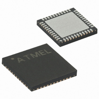
ATMEGA32A-MNR Atmel, ATMEGA32A-MNR Datasheet - Page 81

ATMEGA32A-MNR
Manufacturer Part Number
ATMEGA32A-MNR
Description
IC MCU AVR 32K 16MHZ 44VQFN
Manufacturer
Atmel
Series
AVR® ATmegar
Datasheet
1.ATMEGA32A-MU.pdf
(353 pages)
Specifications of ATMEGA32A-MNR
Core Processor
AVR
Core Size
8-Bit
Speed
16MHz
Connectivity
I²C, SPI, UART/USART
Peripherals
Brown-out Detect/Reset, POR, PWM, WDT
Number Of I /o
32
Program Memory Size
32KB (16K x 16)
Program Memory Type
FLASH
Eeprom Size
1K x 8
Ram Size
2K x 8
Voltage - Supply (vcc/vdd)
2.7 V ~ 5.5 V
Data Converters
A/D 8x10b
Oscillator Type
Internal
Operating Temperature
-40°C ~ 85°C
Package / Case
44-VFQFN Exposed Pad
Lead Free Status / RoHS Status
Lead free / RoHS Compliant
Available stocks
Company
Part Number
Manufacturer
Quantity
Price
- Current page: 81 of 353
- Download datasheet (6Mb)
8155C–AVR–02/11
The PWM resolution for the phase correct PWM mode is fixed to eight bits. In phase correct
PWM mode the counter is incremented until the counter value matches MAX. When the counter
reaches MAX, it changes the count direction. The TCNT0 value will be equal to MAX for one
timer clock cycle. The timing diagram for the phase correct PWM mode is shown on
The TCNT0 value is in the timing diagram shown as a histogram for illustrating the dual-slope
operation. The diagram includes non-inverted and inverted PWM outputs. The small horizontal
line marks on the TCNT0 slopes represent compare matches between OCR0 and TCNT0.
Figure 14-7. Phase Correct PWM Mode, Timing Diagram
The Timer/Counter Overflow Flag (TOV0) is set each time the counter reaches BOTTOM. The
Interrupt Flag can be used to generate an interrupt each time the counter reaches the BOTTOM
value.
In phase correct PWM mode, the compare unit allows generation of PWM waveforms on the
OC0 pin. Setting the COM01:0 bits to 2 will produce a non-inverted PWM. An inverted PWM out-
put can be generated by setting the COM01:0 to 3 (see
value will only be visible on the port pin if the data direction for the port pin is set as output. The
PWM waveform is generated by clearing (or setting) the OC0 Register at the compare match
between OCR0 and TCNT0 when the counter increments, and setting (or clearing) the OC0
Register at compare match between OCR0 and TCNT0 when the counter decrements. The
PWM frequency for the output when using phase correct PWM can be calculated by the follow-
ing equation:
The N variable represents the prescale factor (1, 8, 64, 256, or 1024).
The extreme values for the OCR0 Register represent special cases when generating a PWM
waveform output in the phase correct PWM mode. If the OCR0 is set equal to BOTTOM, the out-
TCNTn
OCn
OCn
Period
1
f
OCnPCPWM
2
=
----------------- -
N 510
f
clk_I/O
⋅
Table 14-5 on page
3
OCn Interrupt Flag Set
OCRn Update
TOVn Interrupt Flag Set
ATmega32A
(COMn1:0 = 2)
(COMn1:0 = 3)
86). The actual OC0
Figure
14-7.
81
Related parts for ATMEGA32A-MNR
Image
Part Number
Description
Manufacturer
Datasheet
Request
R

Part Number:
Description:
Manufacturer:
Atmel Corporation
Datasheet:

Part Number:
Description:
Manufacturer:
ATMEL Corporation
Datasheet:

Part Number:
Description:
IC AVR MCU 32K 16MHZ 5V 44-QFN
Manufacturer:
Atmel
Datasheet:

Part Number:
Description:
IC AVR MCU 32K 16MHZ 5V 40DIP
Manufacturer:
Atmel
Datasheet:

Part Number:
Description:
IC AVR MCU 32K 16MHZ 5V 44TQFP
Manufacturer:
Atmel
Datasheet:

Part Number:
Description:
IC AVR MCU 32K 16MHZ IND 40-DIP
Manufacturer:
Atmel
Datasheet:

Part Number:
Description:
IC AVR MCU 32K 16MHZ IND 44-TQFP
Manufacturer:
Atmel
Datasheet:

Part Number:
Description:
MCU AVR 32KB FLASH 16MHZ 44TQFP
Manufacturer:
Atmel
Datasheet:

Part Number:
Description:
MCU AVR 32KB FLASH 16MHZ 44QFN
Manufacturer:
Atmel
Datasheet:

Part Number:
Description:
MCU AVR 32K FLASH 16MHZ 44-TQFP
Manufacturer:
Atmel
Datasheet:

Part Number:
Description:
IC AVR MCU 32K 16MHZ COM 40-DIP
Manufacturer:
Atmel
Datasheet:

Part Number:
Description:
IC AVR MCU 32K 16MHZ COM 44-QFN
Manufacturer:
Atmel
Datasheet:

Part Number:
Description:
IC AVR MCU 32K 16MHZ COM 44-TQFP
Manufacturer:
Atmel
Datasheet:


