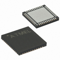
ATMEGA32A-MNR Atmel, ATMEGA32A-MNR Datasheet - Page 123

ATMEGA32A-MNR
Manufacturer Part Number
ATMEGA32A-MNR
Description
IC MCU AVR 32K 16MHZ 44VQFN
Manufacturer
Atmel
Series
AVR® ATmegar
Datasheet
1.ATMEGA32A-MU.pdf
(353 pages)
Specifications of ATMEGA32A-MNR
Core Processor
AVR
Core Size
8-Bit
Speed
16MHz
Connectivity
I²C, SPI, UART/USART
Peripherals
Brown-out Detect/Reset, POR, PWM, WDT
Number Of I /o
32
Program Memory Size
32KB (16K x 16)
Program Memory Type
FLASH
Eeprom Size
1K x 8
Ram Size
2K x 8
Voltage - Supply (vcc/vdd)
2.7 V ~ 5.5 V
Data Converters
A/D 8x10b
Oscillator Type
Internal
Operating Temperature
-40°C ~ 85°C
Package / Case
44-VFQFN Exposed Pad
Lead Free Status / RoHS Status
Lead free / RoHS Compliant
Available stocks
Company
Part Number
Manufacturer
Quantity
Price
- Current page: 123 of 353
- Download datasheet (6Mb)
17.6
17.6.1
8155C–AVR–02/11
Compare Match Output Unit
Compare Output Mode and Waveform Generation
The setup of the OC2 should be performed before setting the Data Direction Register for the port
pin to output. The easiest way of setting the OC2 value is to use the Force Output Compare
(FOC2) strobe bit in Normal mode. The OC2 Register keeps its value even when changing
between Waveform Generation modes.
Be aware that the COM2[1:0] bits are not double buffered together with the compare value.
Changing the COM2[1:0] bits will take effect immediately.
The Compare Output mode (COM21:0) bits have two functions. The Waveform Generator uses
the COM2[1:0] bits for defining the Output Compare (OC2) state at the next compare match.
Also, the COM2[1:0] bits control the OC2 pin output source.
schematic of the logic affected by the COM2[1:0] bit setting. The I/O Registers, I/O bits, and I/O
pins in the figure are shown in bold. Only the parts of the general I/O Port Control Registers
(DDR and PORT) that are affected by the COM2[1:0] bits are shown. When referring to the OC2
state, the reference is for the internal OC2 Register, not the OC2 pin.
Figure 17-4. Compare Match Output Unit, Schematic
The general I/O port function is overridden by the Output Compare (OC2) from the waveform
generator if either of the COM2[1:0] bits are set. However, the OC2 pin direction (input or output)
is still controlled by the Data Direction Register (DDR) for the port pin. The Data Direction Regis-
ter bit for the OC2 pin (DDR_OC2) must be set as output before the OC2 value is visible on the
pin. The port override function is independent of the Waveform Generation mode.
The design of the output compare pin logic allows initialization of the OC2 state before the out-
put is enabled. Note that some COM2[1:0] bit settings are reserved for certain modes of
operation.
The waveform generator uses the COM2[1:0] bits differently in Normal, CTC, and PWM modes.
For all modes, setting the COM2[1:0] = 0 tells the Waveform Generator that no action on the
OC2 Register is to be performed on the next compare match. For compare output actions in the
non-PWM modes refer to
page
134, and for phase correct PWM refer to
“Register Description” on page 132
COMn1
COMn0
FOCn
clk
I/O
Table 17-3 on page
Waveform
Generator
D
D
D
PORT
DDR
OCn
Table 17-5 on page
133. For fast PWM mode, refer to
Q
Q
Q
1
0
Figure 17-4
134.
ATmega32A
OCn
Pin
shows a simplified
Table 17-4 on
123
Related parts for ATMEGA32A-MNR
Image
Part Number
Description
Manufacturer
Datasheet
Request
R

Part Number:
Description:
Manufacturer:
Atmel Corporation
Datasheet:

Part Number:
Description:
Manufacturer:
ATMEL Corporation
Datasheet:

Part Number:
Description:
IC AVR MCU 32K 16MHZ 5V 44-QFN
Manufacturer:
Atmel
Datasheet:

Part Number:
Description:
IC AVR MCU 32K 16MHZ 5V 40DIP
Manufacturer:
Atmel
Datasheet:

Part Number:
Description:
IC AVR MCU 32K 16MHZ 5V 44TQFP
Manufacturer:
Atmel
Datasheet:

Part Number:
Description:
IC AVR MCU 32K 16MHZ IND 40-DIP
Manufacturer:
Atmel
Datasheet:

Part Number:
Description:
IC AVR MCU 32K 16MHZ IND 44-TQFP
Manufacturer:
Atmel
Datasheet:

Part Number:
Description:
MCU AVR 32KB FLASH 16MHZ 44TQFP
Manufacturer:
Atmel
Datasheet:

Part Number:
Description:
MCU AVR 32KB FLASH 16MHZ 44QFN
Manufacturer:
Atmel
Datasheet:

Part Number:
Description:
MCU AVR 32K FLASH 16MHZ 44-TQFP
Manufacturer:
Atmel
Datasheet:

Part Number:
Description:
IC AVR MCU 32K 16MHZ COM 40-DIP
Manufacturer:
Atmel
Datasheet:

Part Number:
Description:
IC AVR MCU 32K 16MHZ COM 44-QFN
Manufacturer:
Atmel
Datasheet:

Part Number:
Description:
IC AVR MCU 32K 16MHZ COM 44-TQFP
Manufacturer:
Atmel
Datasheet:


