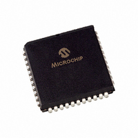
PIC16F874-20/L Microchip Technology, PIC16F874-20/L Datasheet - Page 103

PIC16F874-20/L
Manufacturer Part Number
PIC16F874-20/L
Description
IC MCU FLASH 4KX14 EE 44PLCC
Manufacturer
Microchip Technology
Series
PIC® 16Fr
Datasheets
1.PIC16F616T-ISL.pdf
(8 pages)
2.PIC16F688T-ISL.pdf
(688 pages)
3.PIC16F873-04SO.pdf
(218 pages)
4.PIC16F873-04SO.pdf
(5 pages)
5.PIC16F873-04SO.pdf
(5 pages)
Specifications of PIC16F874-20/L
Core Size
8-Bit
Program Memory Size
7KB (4K x 14)
Core Processor
PIC
Speed
20MHz
Connectivity
I²C, SPI, UART/USART
Peripherals
Brown-out Detect/Reset, POR, PWM, WDT
Number Of I /o
33
Program Memory Type
FLASH
Eeprom Size
128 x 8
Ram Size
192 x 8
Voltage - Supply (vcc/vdd)
4 V ~ 5.5 V
Data Converters
A/D 8x10b
Oscillator Type
External
Operating Temperature
0°C ~ 70°C
Package / Case
44-PLCC
Controller Family/series
PIC16F
No. Of I/o's
33
Eeprom Memory Size
128Byte
Ram Memory Size
192Byte
Cpu Speed
20MHz
No. Of Timers
3
Processor Series
PIC16F
Core
PIC
Data Bus Width
8 bit
Data Ram Size
192 B
Interface Type
MSSP, PSP, USART
Maximum Clock Frequency
20 MHz
Number Of Programmable I/os
33
Number Of Timers
3
Operating Supply Voltage
2 V to 5.5 V
Maximum Operating Temperature
+ 70 C
Mounting Style
SMD/SMT
3rd Party Development Tools
52715-96, 52716-328, 52717-734
Development Tools By Supplier
PG164130, DV164035, DV244005, DV164005, PG164120, ICE2000, DM163022, DV164120
Minimum Operating Temperature
0 C
On-chip Adc
10 bit, 8 Channel
Lead Free Status / RoHS Status
Lead free / RoHS Compliant
For Use With
AC164309 - MODULE SKT FOR PM3 44PLCC444-1001 - DEMO BOARD FOR PICMICRO MCUDVA16XL441 - ADAPTER DEVICE ICE 44PLCC309-1040 - ADAPTER 44-PLCC ZIF TO 40-DIP309-1039 - ADAPTER 44-PLCC TO 40-DIPDV007003 - PROGRAMMER UNIVERSAL PROMATE II
Lead Free Status / Rohs Status
Details
Available stocks
Company
Part Number
Manufacturer
Quantity
Price
Company:
Part Number:
PIC16F874-20/L
Manufacturer:
Microchip Technology
Quantity:
10 000
- PIC16F616T-ISL PDF datasheet
- PIC16F688T-ISL PDF datasheet #2
- PIC16F873-04SO PDF datasheet #3
- PIC16F873-04SO PDF datasheet #4
- PIC16F873-04SO PDF datasheet #5
- Current page: 103 of 688
- Download datasheet (3Mb)
6.3.3
1997 Microchip Technology Inc.
Banking
The data memory is partitioned into four banks. Each bank contains General Purpose Registers
and Special Function Registers. Switching between these banks requires the RP0 and RP1 bits
in the STATUS register to be configured for the desired bank when using direct addressing. The
IRP bit in the STATUS register is used for indirect addressing.
Table 6-1:
Each Bank extends up to 7Fh (128 bytes). The lower locations of each bank are reserved for the
Special Function Registers. Above the Special Function Registers are General Purpose Regis-
ters. All data memory is implemented as static RAM. All Banks may contain special function reg-
isters. Some “high use” special function registers from Bank0 are mirrored in the other banks for
code reduction and quicker access.
Through the evolution of the products, there are a few variations in the layout of the Data Memory.
The data memory organization that will be the standard for all new devices is shown in
Figure
reduce the software overhead for context switching. The registers in bold will be in every device.
The other registers are peripheral dependent. Not every peripheral’s registers are shown,
because some file addresses have a different registers from those shown. As with all the figures,
tables, and specifications presented in this reference guide, verify the details with the device spe-
cific data sheet.
Figure 6-4: Direct Addressing
Accessed
Bank
RP1 RP0
bank select
0
1
2
3
6-5. This Memory map has the last 16-bytes mapped across all memory banks. This is to
Section 6. Memory Organization
Direct and Indirect Addressing of Banks
(RP1:RP0)
Direct
location select
6
Direct Addressing
0 0
0 1
1 0
1 1
Data
Memory
from opcode
Indirect
(IRP)
7Fh
00h
0
1
Bank0
00
0
Bank1
01
Bank2
10
Bank3
11
DS31006A-page 6-9
7Fh
6
Related parts for PIC16F874-20/L
Image
Part Number
Description
Manufacturer
Datasheet
Request
R

Part Number:
Description:
IC MCU FLASH 4KX14 EE 40DIP
Manufacturer:
Microchip Technology
Datasheet:

Part Number:
Description:
IC MCU FLASH 4KX14 EE 40DIP
Manufacturer:
Microchip Technology
Datasheet:

Part Number:
Description:
IC MCU FLASH 4KX14 EE 44PLCC
Manufacturer:
Microchip Technology
Datasheet:

Part Number:
Description:
IC MCU FLASH 4KX14 EE 44TQFP
Manufacturer:
Microchip Technology
Datasheet:

Part Number:
Description:
IC MCU FLASH 4KX14 EE 40DIP
Manufacturer:
Microchip Technology
Datasheet:

Part Number:
Description:
IC,MICROCONTROLLER,8-BIT,PIC CPU,CMOS,QFP,44PIN,PLASTIC
Manufacturer:
Microchip Technology
Datasheet:

Part Number:
Description:
IC MCU FLASH 4KX14 EE 44PLCC
Manufacturer:
Microchip Technology
Datasheet:

Part Number:
Description:
IC MCU FLASH 4KX14 EE 44TQFP
Manufacturer:
Microchip Technology
Datasheet:

Part Number:
Description:
IC MCU FLASH 4KX14 EE 44MQFP
Manufacturer:
Microchip Technology
Datasheet:

Part Number:
Description:
IC MCU FLASH 4KX14 EE 44TQFP
Manufacturer:
Microchip Technology
Datasheet:

Part Number:
Description:
IC MCU FLASH 4KX14 EE 40DIP
Manufacturer:
Microchip Technology
Datasheet:

Part Number:
Description:
IC MCU FLASH 4KX14 EE 44-MQFP
Manufacturer:
Microchip Technology
Datasheet:

Part Number:
Description:
IC MCU FLASH 4KX14 EE 40DIP
Manufacturer:
Microchip Technology
Datasheet:

Part Number:
Description:
IC MCU FLASH 4KX14 EE 44PLCC
Manufacturer:
Microchip Technology
Datasheet:

Part Number:
Description:
IC MCU FLASH 4KX14 EE 44PLCC
Manufacturer:
Microchip Technology
Datasheet:


