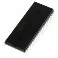
ST72F324BJ6B6 STMicroelectronics, ST72F324BJ6B6 Datasheet - Page 92

ST72F324BJ6B6
Manufacturer Part Number
ST72F324BJ6B6
Description
MCU 8BIT 32KB FLASH/ROM 42-SDIP
Manufacturer
STMicroelectronics
Series
ST7r
Datasheet
1.ST72F324BJ6B6.pdf
(193 pages)
Specifications of ST72F324BJ6B6
Core Processor
ST7
Core Size
8-Bit
Speed
8MHz
Connectivity
SCI, SPI
Peripherals
LVD, POR, PWM, WDT
Number Of I /o
32
Program Memory Size
32KB (32K x 8)
Program Memory Type
FLASH
Ram Size
1K x 8
Voltage - Supply (vcc/vdd)
3.8 V ~ 5.5 V
Data Converters
A/D 12x10b
Oscillator Type
Internal
Operating Temperature
-40°C ~ 85°C
Package / Case
42-SDIP (0.600", 15.24mm)
Controller Family/series
ST7
No. Of I/o's
32
Ram Memory Size
1KB
Cpu Speed
8MHz
No. Of Timers
2
Embedded Interface Type
SCI, SPI
No. Of Pwm Channels
3
Processor Series
ST72F3x
Core
ST7
Data Bus Width
8 bit
Data Ram Size
1 KB
Interface Type
SCI, SPI
Maximum Clock Frequency
8 MHz
Number Of Programmable I/os
32
Number Of Timers
3
Maximum Operating Temperature
+ 85 C
Mounting Style
Through Hole
Development Tools By Supplier
ST7232X-EVAL, ST7MDT20-DVP3, ST7MDT20J-EMU3, STX-RLINK
Minimum Operating Temperature
- 40 C
On-chip Adc
10 bit, 12 Channel
For Use With
497-6421 - BOARD EVAL DGTL BATT CHGR DESIGN497-5046 - KIT TOOL FOR ST7/UPSD/STR7 MCU
Lead Free Status / RoHS Status
Lead free / RoHS Compliant
Eeprom Size
-
Lead Free Status / Rohs Status
Details
Other names
497-5589-5
- Current page: 92 of 193
- Download datasheet (3Mb)
On-chip peripherals
92/193
Table 51.
Input capture 1 high register (IC1HR)
This is an 8-bit register that contains the high part of the counter value (transferred by the
input capture 1 event).
IC1HR
1:0
Bit Name
6
5
4
3
2
MSB
RO
7
OCF1
OCF2
TIMD
ICF2
TOF
-
Output compare flag 1
Timer overflow flag
Input capture flag 2
Output compare flag 2
Timer disable
Reserved, must be kept cleared.
CSR register description (continued)
0: No match (reset value).
1: The content of the free running counter has matched the content of the OC1R
register. To clear this bit, first read the SR register, then read or write the low byte of
the OC1R (OC1LR) register.
0: No timer overflow (reset value).
1: The free running counter rolled over from FFFFh to 0000h. To clear this bit, first
read the SR register, then read or write the low byte of the CR (CLR) register.
Note: Reading or writing the ACLR register does not clear TOF.
0: No input capture (reset value).
1: An Input Capture has occurred on the ICAP2 pin. To clear this bit, first read the SR
register, then read or write the low byte of the IC2R (IC2LR) register.
0: No match (reset value).
1: The content of the free running counter has matched the content of the OC2R
register. To clear this bit, first read the SR register, then read or write the low byte of
the OC2R (OC2LR) register.
This bit is set and cleared by software. When set, it freezes the timer prescaler and
counter and disabled the output functions (OCMP1 and OCMP2 pins) to reduce
power consumption. Access to the timer registers is still available, allowing the timer
configuration to be changed, or the counter reset, while it is disabled.
0: Timer enabled.
1: Timer prescaler, counter and outputs disabled.
RO
6
RO
5
RO
4
Function
RO
3
RO
2
Reset value: undefined
RO
1
ST72324Bxx
LSB
RO
0
Related parts for ST72F324BJ6B6
Image
Part Number
Description
Manufacturer
Datasheet
Request
R

Part Number:
Description:
STMicroelectronics [RIPPLE-CARRY BINARY COUNTER/DIVIDERS]
Manufacturer:
STMicroelectronics
Datasheet:

Part Number:
Description:
STMicroelectronics [LIQUID-CRYSTAL DISPLAY DRIVERS]
Manufacturer:
STMicroelectronics
Datasheet:

Part Number:
Description:
BOARD EVAL FOR MEMS SENSORS
Manufacturer:
STMicroelectronics
Datasheet:

Part Number:
Description:
NPN TRANSISTOR POWER MODULE
Manufacturer:
STMicroelectronics
Datasheet:

Part Number:
Description:
TURBOSWITCH ULTRA-FAST HIGH VOLTAGE DIODE
Manufacturer:
STMicroelectronics
Datasheet:

Part Number:
Description:
Manufacturer:
STMicroelectronics
Datasheet:

Part Number:
Description:
DIODE / SCR MODULE
Manufacturer:
STMicroelectronics
Datasheet:

Part Number:
Description:
DIODE / SCR MODULE
Manufacturer:
STMicroelectronics
Datasheet:

Part Number:
Description:
Search -----> STE16N100
Manufacturer:
STMicroelectronics
Datasheet:

Part Number:
Description:
Search ---> STE53NA50
Manufacturer:
STMicroelectronics
Datasheet:

Part Number:
Description:
NPN Transistor Power Module
Manufacturer:
STMicroelectronics
Datasheet:


