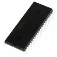
ST72F324BJ6B6 STMicroelectronics, ST72F324BJ6B6 Datasheet - Page 153

ST72F324BJ6B6
Manufacturer Part Number
ST72F324BJ6B6
Description
MCU 8BIT 32KB FLASH/ROM 42-SDIP
Manufacturer
STMicroelectronics
Series
ST7r
Datasheet
1.ST72F324BJ6B6.pdf
(193 pages)
Specifications of ST72F324BJ6B6
Core Processor
ST7
Core Size
8-Bit
Speed
8MHz
Connectivity
SCI, SPI
Peripherals
LVD, POR, PWM, WDT
Number Of I /o
32
Program Memory Size
32KB (32K x 8)
Program Memory Type
FLASH
Ram Size
1K x 8
Voltage - Supply (vcc/vdd)
3.8 V ~ 5.5 V
Data Converters
A/D 12x10b
Oscillator Type
Internal
Operating Temperature
-40°C ~ 85°C
Package / Case
42-SDIP (0.600", 15.24mm)
Controller Family/series
ST7
No. Of I/o's
32
Ram Memory Size
1KB
Cpu Speed
8MHz
No. Of Timers
2
Embedded Interface Type
SCI, SPI
No. Of Pwm Channels
3
Processor Series
ST72F3x
Core
ST7
Data Bus Width
8 bit
Data Ram Size
1 KB
Interface Type
SCI, SPI
Maximum Clock Frequency
8 MHz
Number Of Programmable I/os
32
Number Of Timers
3
Maximum Operating Temperature
+ 85 C
Mounting Style
Through Hole
Development Tools By Supplier
ST7232X-EVAL, ST7MDT20-DVP3, ST7MDT20J-EMU3, STX-RLINK
Minimum Operating Temperature
- 40 C
On-chip Adc
10 bit, 12 Channel
For Use With
497-6421 - BOARD EVAL DGTL BATT CHGR DESIGN497-5046 - KIT TOOL FOR ST7/UPSD/STR7 MCU
Lead Free Status / RoHS Status
Lead free / RoHS Compliant
Eeprom Size
-
Lead Free Status / Rohs Status
Details
Other names
497-5589-5
- Current page: 153 of 193
- Download datasheet (3Mb)
ST72324Bxx
Note:
12.6.5
12.7
12.7.1
To reduce disturbance to the RC oscillator, it is recommended to place decoupling
capacitors between V
PLL characteristics
Table 99.
1. Data characterized but not tested
The user must take the PLL jitter into account in the application (for example in serial
communication or sampling of high frequency signals). The PLL jitter is a periodic effect,
which is integrated over several CPU cycles. Therefore the longer the period of the
application signal, the less it will be impacted by the PLL jitter.
Figure 69
2 MHz. At frequencies of less than 125 kHz, the jitter is negligible.
Figure 69. Integrated PLL jitter vs signal frequency
1. Measurement conditions: f
Memory characteristics
RAM and hardware registers
Table 100. RAM and hardware registers
1. Minimum V
Δ f
Symbol
Symbol
hardware registers (only in Halt mode). Not tested in production.
V
CPU
f
RM
OSC
/f
CPU
shows the PLL jitter integrated on application signals in the range 125 kHz to
Data retention mode
DD
PLL characteristics
PLL input frequency range
Instantaneous PLL jitter
supply voltage without losing data stored in RAM (in Halt mode or under reset) or in
Parameter
DD
Parameter
CPU
+/-Jitter (%)
and V
= 8 MHz
1.2
0.8
0.6
0.4
0.2
1
0
(1)
SS
4 MHz
as shown in
(1)
2 MHz
Halt mode (or reset)
Application Frequency
f
1 MHz 500 kHz 250 kHz 125 kHz
OSC
Conditions
Figure 87 on page
Conditions
= 4 MHz
(1)
Max
Typ
Min
1.6
Min
2
Electrical characteristics
170.
Typ
Typ
0.7
Max
Max
4
2
153/193
MHz
Unit
Unit
%
V
Related parts for ST72F324BJ6B6
Image
Part Number
Description
Manufacturer
Datasheet
Request
R

Part Number:
Description:
STMicroelectronics [RIPPLE-CARRY BINARY COUNTER/DIVIDERS]
Manufacturer:
STMicroelectronics
Datasheet:

Part Number:
Description:
STMicroelectronics [LIQUID-CRYSTAL DISPLAY DRIVERS]
Manufacturer:
STMicroelectronics
Datasheet:

Part Number:
Description:
BOARD EVAL FOR MEMS SENSORS
Manufacturer:
STMicroelectronics
Datasheet:

Part Number:
Description:
NPN TRANSISTOR POWER MODULE
Manufacturer:
STMicroelectronics
Datasheet:

Part Number:
Description:
TURBOSWITCH ULTRA-FAST HIGH VOLTAGE DIODE
Manufacturer:
STMicroelectronics
Datasheet:

Part Number:
Description:
Manufacturer:
STMicroelectronics
Datasheet:

Part Number:
Description:
DIODE / SCR MODULE
Manufacturer:
STMicroelectronics
Datasheet:

Part Number:
Description:
DIODE / SCR MODULE
Manufacturer:
STMicroelectronics
Datasheet:

Part Number:
Description:
Search -----> STE16N100
Manufacturer:
STMicroelectronics
Datasheet:

Part Number:
Description:
Search ---> STE53NA50
Manufacturer:
STMicroelectronics
Datasheet:

Part Number:
Description:
NPN Transistor Power Module
Manufacturer:
STMicroelectronics
Datasheet:


