HDJD-JD05 Avago Technologies US Inc., HDJD-JD05 Datasheet - Page 9
HDJD-JD05
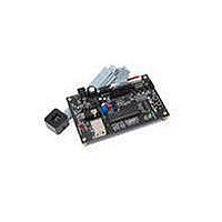
Manufacturer Part Number
HDJD-JD05
Description
KIT DEV RGB COLOR SENSOR 20-QFN
Manufacturer
Avago Technologies US Inc.
Specifications of HDJD-JD05
Sensor Type
Light, Color Sensor
Sensing Range
RGB
Interface
2-Wire Serial
Voltage - Supply
2.5 V ~ 3.6 V
Embedded
No
Utilized Ic / Part
ADJD-S313-QR999
For Use With/related Products
ADJD-S313-QR999
Lead Free Status / RoHS Status
Not applicable / Not applicable


The SCL clock line synchronizes the serial data
transmission on the SDA data line. It is always
generated by the master. The frequency of the SCL
clock line may vary throughout the transmission as
long as it still meets the minimum timing
requirements.
The master by default drives the SDA data line. The
slave drives the SDA data line only when sending
an acknowledge bit after the master writes data to
the slave or when the master requests the slave to
send data.
The SDA data line driven by the master may be
implemented on the negative edge of the SCL clock
line. The master may sample data driven by the
slave on the positive edge of the SCL clock line.
Figure
implementation and how the SCL clock line and
SDA data line can be synchronized.
A complete data transfer is 8-bits long or 1-byte.
Each byte is sent most significant bit (MSB) first
followed by an acknowledge or not acknowledge
bit. Each data transfer can send an unlimited
number of bytes (depending on the data format).
Figure 4. Data Byte Transfer
Figure 5. Slave-Receiver Acknowledge
(MASTER-TRANSMITTER)
9
SDA
SCL
START or repeated
START condition
(SLAVE-RECEIVER)
Sr
or
S
shows an example of a master
(MASTER)
MSB
1
SDA
SDA
SCL
2
LSB
8
SDA pulled LOW
LSB
8
by receiver
ACK
9
Figure 3. Data Bit Synchronization
Acknowledge/Not acknowledge
The receiver must always acknowledge each byte
sent in a data transfer. In the case of the slave-
receiver and master-transmitter, if the slave-
receiver does not send an acknowledge bit, the
master-transmitter can either STOP the transfer or
generate a repeated START to start a new transfer.
SDA
SCL
MSB
1
2
SDA left HIGH
by transmitter
Acknowledge
Acknowledge
clock pulse
SDA data sampled on the
positive edge of SCL
9
LSB
8
SDA data driven on the
negative edge of SCL
ACK
NO
STOP or repeated
START condition
9
Sr
or
P
Sr
P
Related parts for HDJD-JD05
Image
Part Number
Description
Manufacturer
Datasheet
Request
R

Part Number:
Description:
KIT DEV RGB COLOR SENSOR 16-QFN
Manufacturer:
Avago Technologies US Inc.
Datasheet:

Part Number:
Description:
KIT DEV RGB COLOR SENSOR 16-QFN
Manufacturer:
Avago Technologies US Inc.
Datasheet:

Part Number:
Description:
KIT DEV RGB DCS 2.2X2.2
Manufacturer:
Avago Technologies US Inc.
Datasheet:

Part Number:
Description:
Optical Sensor
Manufacturer:
Avago Technologies US Inc.
Datasheet:
Part Number:
Description:
RGB COLOR CONTROLLER AND SENSOR
Manufacturer:
Avago Technologies US Inc.
Part Number:
Description:
Photodiodes Color Controller
Manufacturer:
Avago Technologies US Inc.

Part Number:
Description:
Optical Sensors - Board Mount RGB Color Sensor
Manufacturer:
Avago Technologies US Inc.

Part Number:
Description:
Optical Sensors - Board Mount RGB Color Sensor
Manufacturer:
Avago Technologies US Inc.

Part Number:
Description:
Optical Sensor Development Tools RGB CONTROLLER Development Kit
Manufacturer:
Avago Technologies US Inc.

Part Number:
Description:
Optical Sensor Development Tools RGB CONTROLLER Development Kit
Manufacturer:
Avago Technologies US Inc.

Part Number:
Description:
OPTOCOUPLER GATE DRV 2A 16-SOIC
Manufacturer:
Avago Technologies US Inc.
Datasheet:
Part Number:
Description:
OPTOCOUPLER 2CH 2.5A 16-SOIC
Manufacturer:
Avago Technologies US Inc.
Datasheet:

Part Number:
Description:
OPTOCOUPLER GATE DRV 0.4A 16SOIC
Manufacturer:
Avago Technologies US Inc.
Datasheet:

Part Number:
Description:
OPTOCOUPLER 2.0A 250KHZ 8-DIP
Manufacturer:
Avago Technologies US Inc.
Datasheet:

Part Number:
Description:
OPTOCOUPLER 2.0A 250KHZ GW 8-SMD
Manufacturer:
Avago Technologies US Inc.
Datasheet: