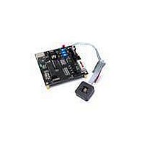
HDJD-JD06 Avago Technologies US Inc., HDJD-JD06 Datasheet

HDJD-JD06
Specifications of HDJD-JD06
Related parts for HDJD-JD06
HDJD-JD06 Summary of contents
Page 1
... Can also be coupled with Avago Technologies’ patented color controller, HDJD-J822, to form a closed loop color management system ESD WARNING: Standard CMOS handling precautions should be observed to avoid static discharge. THIS PRODUCT IS NOT CERTIFIED OR WARRANTIED FOR AUTOMOTIVE APPLICATIONS. IF THE CUSTOMER INTENDS TO USE IT FOR AUTOMOTIVE APPLICATIONS, THEY THEIR OWN RISK ...
Page 2
Package Dimension Bottom View 0.8 0.30 3.2 5.0±0.15 Note: Dimensions are in millimeters (mm) Part Numbering System ADJD Gain Selection ...
Page 3
Theory of Operation The integral R,G,B color filters on the photodiode array detect the R,G,B components of the light falling on the sensor. The photodiode convert the R,G,B light components into photocurrents. The integrated transimpedence amplifiers for R,G,B components then ...
Page 4
Absolute Maximum Ratings Parameter Supply Voltage Storage Temperature Operating Temperature Human Body Model ESD Rating Machine Model ESD Rating Charge Device Model ESD Rating Note: 1. Subjecting the part to stresses beyond those listed under this section may cause ...
Page 5
Operating Conditions and Electrical Requirements Electrical Characteristics 5V Parameter Sym. Remark Dark voltage Max. output V OMAX voltage swing Supply current GS:111, λ Irradiance Re ...
Page 6
Parameter Sym. Remark GS:101, λ Saturation [5] Irradiance GS:101, λ GS:101, λ GS:100, λ Saturation [5] Irradiance GS:100, λ GS:100, λ GS:011, λ Saturation Irradiance [5] GS: 011, λ GS: 011, λ GS:010, λ Saturation Irradiance [5] GS:010, λ GS:010, ...
Page 7
Gain Selection Feedback Resistor Table GS: Bit 2 GS: Bit 1 Bit 0 Feedback Resistor 5.3 ...
Page 8
Temperature (˚C) Figure 2. Dark Voltage vs Operating Temperature 4.7 4 3.2 2.4 1.6 0 0.5 1 1.5 Irradiance - Ee (mW/cm Figure 3. Voltage Output of Blue Channel vs ...
Page 9
Irradiance - Ee (mW/cm Figure 5. Voltage Output of Red Channel vs Irradiance (lp = 645 nm) Recommended Reflow Profile It is recommended that Henkel Pb-free solder paste LF310 be ...
Page 10
Lead QFN Recommended PCB Land Pad Design IPC-SM-782 is used as the standard for the PCB land- pad design. Recommended PCB finishing is gold plated. 0.4 mm 3.19 mm 5.5 mm 3.19 mm 3.9 5.5 mm Figure 7. Recommendations ...
Page 11
Package Tape and Reel Dimensions Carrier Tape Dimensions 4.00 0.10 SEE NOTE #2 2.00 0.05 SEE NOTE # SECTION B 0.30 0.05 SECTION A-A NOTES AND B ...
Page 12
ESD WARNING: Standard CMOS handling precautions should be observed to avoid static discharge. THIS PRODUCT IS NOT CERTIFIED OR WARRANTIED FOR AUTOMOTIVE APPLICATIONS. IF THE CUSTOMER INTENDS TO USE IT FOR AUTOMOTIVE APPLICATIONS, THEY THEIR OWN RISK. ...


