EVAL-AD5381EB Analog Devices Inc, EVAL-AD5381EB Datasheet - Page 8
EVAL-AD5381EB
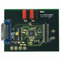
Manufacturer Part Number
EVAL-AD5381EB
Description
BOARD EVAL FOR AD5381
Manufacturer
Analog Devices Inc
Specifications of EVAL-AD5381EB
Rohs Status
RoHS non-compliant
Number Of Dac's
40
Number Of Bits
12
Outputs And Type
40, Single Ended
Sampling Rate (per Second)
167k
Data Interface
DSP, I²C, MICROWIRE™, Parallel, QSPI™, SPI™
Settling Time
6µs
Dac Type
Voltage
Voltage Supply Source
Single
Operating Temperature
-40°C ~ 85°C
Utilized Ic / Part
AD5381


AD5381
TIMING CHARACTERISTICS
SERIAL INTERFACE TIMING
DVDD = 2.7 V to 5.5 V; AVDD= 4.5 V to 5.5 V or 2.7 V to 3.6 V; AGND = DGND = 0 V;
all specifications T
Table 6.
Parameter
t
t
t
t
t
t
t
t
t
t
t
t
t
t
t
t
t
t
t
t
t
t
t
t
1
2
3
4
5
1
2
3
4
5
6
7
7A
8
9
10
11
12
13
14
15
16
17
18
19
20
21
22
23
Guaranteed by design and characterization, not production tested.
All input signals are specified with t
See Figure 2, Figure 3, Figure 4, and Figure 5.
Standalone mode only.
Daisy-chain mode only.
4
4
4
4
5
5
5
1, , 2 3
MIN
to T
Limit at T
33
13
13
13
13
33
10
50
5
4.5
30
670
20
20
100
0
100
8
20
12
20
5
8
20
MAX
, unless otherwise noted.
r
= t
f
= 5 ns (10% to 90% of V
MIN
, T
MAX
TO OUTPUT PIN
Figure 2. Load Circuit for Digital Output Timing
CC
Unit
ns min
ns min
ns min
ns min
ns min
ns min
ns min
ns min
ns min
ns min
ns max
ns max
ns min
ns min
ns max
ns min
ns min
μs typ
ns min
μs max
ns max
ns min
ns min
ns min
) and are timed from a voltage level of 1.2 V.
Rev. B | Page 8 of 40
C
50pF
L
200μA
200μA
Description
SCLK cycle time
SCLK high time
SCLK low time
SYNC falling edge to SCLK falling edge setup time
24
Minimum SYNC low time
Minimum SYNC high time
Minimum SYNC high time in Readback mode
Data setup time
Data hold time
24
BUSY pulse width low (single channel update)
24th SCLK falling edge to LDAC falling edge
LDAC pulse width low
BUSY rising edge to DAC output response time
BUSY rising edge to LDAC falling edge
LDAC falling edge to DAC output response time
DAC output settling time
CLR pulse width low
CLR pulse activation time
SCLK rising edge to SDO valid
SCLK falling edge to SYNC rising edge
SYNC rising edge to SCLK rising edge
SYNC rising edge to LDAC falling edge
th
th
SCLK falling edge to SYNC falling edge
SCLK falling edge to BUSY falling edge
I
I
OL
OH
V
V
OH
OL
(MAX)
(MIN) OR
Related parts for EVAL-AD5381EB
Image
Part Number
Description
Manufacturer
Datasheet
Request
R

Part Number:
Description:
ENERCHIP CC EVAL KIT
Manufacturer:
Cymbet Corporation
Datasheet:

Part Number:
Description:
BOARD EVAL FOR AD976
Manufacturer:
Analog Devices Inc
Datasheet:

Part Number:
Description:
BOARD EVAL FOR ADXL345
Manufacturer:
Analog Devices Inc
Datasheet:

Part Number:
Description:
ENERCHIP CC SEH EVAL KIT
Manufacturer:
Cymbet Corporation
Datasheet:

Part Number:
Description:
ENERCHIP EP ENERGY HARVEST EVAL
Manufacturer:
Cymbet Corporation
Datasheet:

Part Number:
Description:
EVAL BOARD FOR TW6864-LB2-GR
Manufacturer:
Intersil
Datasheet:
Part Number:
Description:
EVAL BOARD FOR TW8816-LB3-GR
Manufacturer:
Intersil
Datasheet:
Part Number:
Description:
EVAL BOARD FOR TW8817-TA3-GRS
Manufacturer:
Intersil
Datasheet:

Part Number:
Description:
EVALUATION MODULE FOR ADUM4160
Manufacturer:
Analog Devices Inc
Datasheet:

Part Number:
Description:
BOARD EVALUATION ADCMP581BCP
Manufacturer:
Analog Devices Inc
Datasheet:
Part Number:
Description:
BOARD EVALUATION ADM1041
Manufacturer:
Analog Devices Inc
Datasheet:

Part Number:
Description:
EVAL BOARD FOR STM32F107VCT
Manufacturer:
STMicroelectronics
Datasheet:
Part Number:
Description:
BOARD EVAL FOR AD1954
Manufacturer:
Analog Devices Inc
Datasheet:
Part Number:
Description:
BOARD EVAL FOR AD1955
Manufacturer:
Analog Devices Inc
Datasheet:

Part Number:
Description:
BOARD EVAL FOR AD7655
Manufacturer:
Analog Devices Inc
Datasheet: