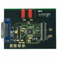
EVAL-AD5381EB Analog Devices Inc, EVAL-AD5381EB Datasheet - Page 7

EVAL-AD5381EB
Manufacturer Part Number
EVAL-AD5381EB
Description
BOARD EVAL FOR AD5381
Manufacturer
Analog Devices Inc
Specifications of EVAL-AD5381EB
Rohs Status
RoHS non-compliant
Number Of Dac's
40
Number Of Bits
12
Outputs And Type
40, Single Ended
Sampling Rate (per Second)
167k
Data Interface
DSP, I²C, MICROWIRE™, Parallel, QSPI™, SPI™
Settling Time
6µs
Dac Type
Voltage
Voltage Supply Source
Single
Operating Temperature
-40°C ~ 85°C
Utilized Ic / Part
AD5381
Parameter
LOGIC OUTPUTS (BUSY, SDO)
LOGIC OUTPUT (SDA)
POWER REQUIREMENTS
1
2
3
4
AC CHARACTERISTICS
AVDD = 4.5 V to 5.5 V or 2.7 V to 3.6 V; DVDD = 2.7 V to 5.5 V; AGND = DGND = 0 V.
Table 5.
Parameter
DYNAMIC PERFORMANCE
1
2
AD5381-3 is calibrated using an external 1.25 V reference. Temperature range is –40°C to +85°C.
Accuracy guaranteed from VOUT = 10 mV to AVDD – 50 mV.
Guaranteed by characterization, not production tested.
Default on the AD5381-3 is 1.25 V. Programmable to 2.5 V via CR10 in the AD5381 control register; operating the AD5381-3 with a 2.5 V reference will lead to degraded
accuracy specifications and limited input code range.
Guaranteed by design and characterization, not production tested.
Slew rate can be programmed via the current boost control bit in the AD5381 control register.
V
V
High Impedance Leakage Current
High Impedance Output Capacitance
V
Three-State Leakage Current
Three-State Output Capacitance
AVDD
DVDD
Power Supply Sensitivity
∆Midscale/∆ΑV
AI
DI
AI
DI
Power Dissipation
Output Voltage Settling Time
Slew Rate
Digital-to-Analog Glitch Energy
Glitch Impulse Peak Amplitude
DAC-to-DAC Crosstalk
Digital Crosstalk
Digital Feedthrough
Output Noise 0.1 Hz to 10 Hz
Output Noise Spectral Density
OL
OH
OL
DD
DD
DD
DD
@ 1 kHz
@ 10 kHz
, Output Low Voltage
, Output Low Voltage
, Output High Voltage
(Power-Down)
(Power-Down)
2
DD
3
3
1
3
All
6
8
2
3
12
15
1
0.8
0.1
15
40
150
100
AD5381-3
0.4
DVDD – 0.5
±1
5
0.4
0.6
±1
8
2.7/3.6
2.7/5.5
–85
0.375
0.475
1
2
20
48
1
Unit
μs typ
μs max
V/μs typ
V/μs typ
nV-s typ
mV typ
nV-s typ
nV-s typ
nV-s typ
μV p-p typ
μV p-p typ
nV/√Hz typ
nV/√Hz typ
Unit
V max
V min
μA max
pF typ
V max
V max
μA max
pF typ
V min/max
V min/max
dB typ
mA/channel max
mA/channel max
mA max
μA max
μA max
mW max
Rev. B | Page 7 of 40
Test Conditions/Comments
1/4 scale to 3/4 scale change settling to ±1 LSB
Boost mode off, CR9 = 0
Boost mode on, CR9 = 1
See Terminology section
Effect of input bus activity on DAC output under test
External reference, midscale loaded to DAC
Internal reference, midscale loaded to DAC
Test Conditions/Comments
Sinking 200 μA
Sourcing 200 μA
SDO only
SDO only
I
I
Outputs unloaded, boost off; 0.25 mA/channel typ
Outputs unloaded, boost on; 0.325 mA/channel typ
V
Outputs unloaded, boost off, AVDD = DVDD = 3 V
SINK
SINK
IH
= DVDD, V
= 3 mA
= 6 mA
IL
= DGND
AD5381


