HS0005KCU01H Renesas Electronics America, HS0005KCU01H Datasheet
HS0005KCU01H
Specifications of HS0005KCU01H


Related parts for HS0005KCU01H


HS0005KCU01H Summary of contents
Page 1
To our customers, Old Company Name in Catalogs and Other Documents st On April 1 , 2010, NEC Electronics Corporation merged with Renesas Technology Corporation, and Renesas Electronics Corporation took over all the business of both companies. Therefore, although the ...
Page 2
All information included in this document is current as of the date this document is issued. Such information, however, is subject to change without any prior notice. Before purchasing or using any Renesas Electronics products listed herein, please confirm ...
Page 3
SuperH™ Family E10A-USB Emulator Additional Document for User’s Manual E10A-USB for SH7329 HS7329KCU01HE Renesas Microcomputer Development Environment System SuperH™ Family Supplementary Information on Using the SH7329 Rev.1.00 2004.10 ...
Page 4
...
Page 5
Keep safety first in your circuit designs! 1. Renesas Technology Corp. puts the maximum effort into making semiconductor products better and more reliable, but there is always the possibility that trouble may occur with them. Trouble with semiconductors may lead ...
Page 6
...
Page 7
Section 1 Connecting the Emulator with the User System ................................1 1.1 Components of the Emulator ............................................................................................ 1 1.2 Connecting the Emulator with the User System ............................................................... 2 1.3 Installing the H-UDI Port Connector on the User System ................................................ 3 1.4 ...
Page 8
ii ...
Page 9
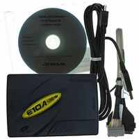
... Family E10A-USB Emulator User’s Manual, Supplementary Information on Using the SH7329*, and Test program manual for HS0005KCU01H and HS0005KCU02H Note: Additional document for the MPUs supported by the emulator is included. Check the target MPU and refer to its additional document. Quan- Appearance tity ...
Page 10
... AUD function. Table 1.2 Type Number, AUD Function, and Connector Type Type Number HS0005KCU02H HS0005KCU01H The H-UDI port connector has the 36-pin and 14-pin types as described below. Use them according to the purpose of the usage. 1. 36-pin type (with AUD function) The AUD trace function is supported. A large amount of trace information can be acquired in realtime ...
Page 11
Installing the H-UDI Port Connector on the User System Table 1.3 shows the recommended H-UDI port connectors for the emulator. Table 1.3 Recommended H-UDI Port Connectors Connector Type Number 36-pin connector DX10M-36S DX10M-36SE, DX10G1M-36SE 14-pin connector 2514-6002 Note: When ...
Page 12
Pin Input/ No. Signal *1 Output AUDCK Output 1 2 GND Output 3 AUDATA0 4 GND Output 5 AUDATA1 6 GND Output AUDATA2 7 8 GND AUDATA3 Output 9 10 GND *2 11 /AUDSYNC Output 12 GND ...
Page 13
Pin No. Signal 1 TCK 2 /TRST *2 3 TDO 4 /ASEBRKAK *2 5 TMS 6 TDI 7 /RESETP * /CA 9 (GND UVCC 10, 12, GND and GND Notes: 1. Input to ...
Page 14
Recommended Circuit between the H-UDI Port Connector and the MPU 1.5.1 Recommended Circuit (36-Pin Type) Figure 1.3 shows a recommended circuit for connection between the H-UDI and AUD port connectors (36 pins) and the MPU when the emulator is ...
Page 15
When the circuit is connected as shown in figure 1.3, the switches of the emulator are set as SW2 = 1 and SW3 = 1. For details, refer to section 3.8, Setting the DIP Switches, in the Debugger Part TM ...
Page 16
Recommended Circuit (14-Pin Type) Figure 1.4 shows a recommended circuit for connection between the H-UDI and AUD port connectors (14 pins) and the MPU when the emulator is in use. Notes not connect anything to the N.C. ...
Page 17
When the circuit is connected as shown in figure 1.4, the switches of the emulator are set as SW2 = 1 and SW3 = 1. For details, refer to section 3.8, Setting the DIP Switches, in the Debugger Part TM ...
Page 18
10 ...
Page 19
Section 2 Software Specifications when Using the SH7329 2.1 Differences between the SH7329 and the Emulator 1. When the emulator system is initiated, it initializes the general registers and part of the control registers as shown in table 2.1. The ...
Page 20
Low-Power States (Sleep, Software Standby, Module Standby, and U Standby) For low-power consumption, the SH7329 has sleep, software standby, module standby, and U standby states. The sleep, software standby, and module standby states are switched using the SLEEP instruction. ...
Page 21
Cache Operation during User Program Break When cache is enabled, the emulator accesses the memory by the following methods: At memory write: Writes through the cache, then writes to the memory. At memory read: Does not change the cache ...
Page 22
... Loading Sessions Information in [JTAG clock] of the [Configuration] dialog box cannot be recovered by loading sessions. Thus the TCK value will be as follows: When HS0005KCU01H or HS0005KCU02H is used: TCK = 0.625 MHz 15. [IO] window Display and modification Do not change values of the User Break Controller because it is used by the emulator. ...
Page 23
The internal I/O registers can be accessed from the [IO] window. However, note the following when accessing the SDMR register of the bus-state controller. Before accessing the SDMR register, specify addresses to be accessed in the I/O-register definition file (SH7329.IO) ...
Page 24
Specific Functions for the Emulator when Using the SH7329 In the SH7329, a reset must be input when the emulator is activated. Do not use the activation method described in section 3.11 in the SuperH 2.2.1 Break Condition Functions ...
Page 25
Note: When U-RAM or X/Y-RAM is accessed from the P0 space, the I-bus must be selected, and when accessed from the P2 space, the L-bus must be selected. When cache fill cycle is acquired, the I-bus must be selected. Table ...
Page 26
... Table 2.7 shows the type numbers that the AUD function can be used. Table 2.7 Type Number and AUD Function Type Number HS0005KCU01H HS0005KCU02H AUD Trace Functions: This function is operational when the AUD pin of the device is connected to the emulator. Table 2.8 shows the AUD trace acquisition mode that can be set in each trace function ...
Page 27
To set the AUD trace acquisition mode, click the [Trace] window with the right mouse button and select [Setting] from the pop-up menu to display the [Acquisition] dialog box. The AUD trace acquisition mode can be set in the [AUD ...
Page 28
Branch Trace Function The branch source and destination addresses and their source lines are displayed. Branch trace can be acquired by selecting the [Branch trace] check box in the [AUD function] group box of the [Trace mode] page. The ...
Page 29
Notes: 1. When the [L-bus] or [I(M)-bus] radio button is selected, the bus cycles listed below will be traced. The [I-bus] and [M-bus] radio buttons are only available when the [I(M)-bus] radio button has been selected. L-bus: A bus cycle ...
Page 30
When U-RAM or X/Y-RAM is accessed from the P0 space, the I-bus must be selected, and when accessed from the P2 space, the L-bus must be selected. When a cache fill cycle is acquired, I-bus must be selected. 2. Address ...
Page 31
Do not use the AUD full-trace mode for the VIO function completion-type exception occurs during exception branch acquisition, the next address to the address in which an exception occurs is acquired. Internal Trace Function: This function ...
Page 32
Conditions set at Break Condition 2 are disabled when an instruction to which a BREAKPOINT has been set is executed. Do not set a BREAKPOINT to an instruction in which Break Condition 2 is satisfied. 5. When execution resumes ...
Page 33
BREAKPOINT setting, the BREAKPOINT address remains unchanged. When a BREAKPOINT is satisfied with the modified address in the VP_MAP table, the cause of termination displayed in the status bar and the [Output] window is ILLEGAL INSTRUCTION, not BREAKPOINT. 13. If ...
Page 34
Performance Measurement Function The emulator supports the performance measurement function. 1. Setting the performance measurement conditions To set the performance measurement conditions, use the [Performance Analysis] dialog box and the PERFORMANCE_SET command. When any line on the [Performance Analysis] ...
Page 35
Figure 2.4 [Performance Analysis] Dialog Box (b) Measurement range One of the following ranges can be specified. This depends on the item selected for [Mode] in the [Performance Analysis] dialog box. 1. From the start to the end of the ...
Page 36
Notes: 1. When the second and third ranges are specified, execute the user program after the measurement start condition is set to Break Condition 1 (or Break Condition 2) and the measurement end condition to Break Condition 2 (or Break ...
Page 37
Table 2.10 Measurement Item Selected Name Disabled Elapsed time Number of execution states Branch instruction counts Number of execution instructions DSP-instruction execution counts Instruction/data conflict cycle Other conflict cycles than instruction/data Exception/interrupt counts Data-TLB miss cycle Instruction-TLB miss cycle Interrupt ...
Page 38
Table 2.10 Measurement Item (cont) Selected Name Cacheable area instruction access cycle Cacheable area data access cycle Access counts other than instruction/data Non-cacheable area access counts Non-cacheable area instruction access counts Non-cacheable area data access counts Cacheable area access counts ...
Page 39
Initializing the measured result To initialize the measured result, select [Initialize] from the popup menu in the [Performance Analysis] window or specify INIT with the PERFORMANCE_ANALYSIS command. 2.2.8 Notes on U Standby State Controlling Vcc (main) in the U ...
Page 40
Figure 2.5 [Recovery Information] Page The following shows the procedures recovered from the U standby state the software standby mode, when the /CA pin is asserted, the emulator enters the U standby state and the message box shown ...
Page 41
... Information] page. If this is not selected, the TCK value will be as follows: When HS0005KCU01H or HS0005KCU02H is used: TCK = 0.625 MHz 3. After the /CA pin has been negated, if /RESETP is not input for about 30 seconds, a timeout error will occur ...
Page 42
34 ...
Page 43
TM SuperH Family E10A-USB Emulator Additional Document for User's Manual Supplementary Information on Using the SH7329 Publication Date: Rev.1.00, October 15, 2004 Published by: Sales Strategic Planning Div. Renesas Technology Corp. Edited by: Technical Documentation & Information Department Renesas Kodaira ...
Page 44
RENESAS SALES OFFICES Refer to "http://www.renesas.com/en/network" for the latest and detailed information. Renesas Technology America, Inc. 450 Holger Way, San Jose, CA 95134-1368, U.S.A Tel: <1> (408) 382-7500, Fax: <1> (408) 382-7501 Renesas Technology Europe Limited Dukes Meadow, Millboard Road, ...
Page 45
SuperH™ Family E10A-USB Emulator Additional Document for User’s Manual 1753, Shimonumabe, Nakahara-ku, Kawasaki-shi, Kanagawa 211-8668 Japan REJ10B0159-0100H ...