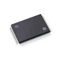
C8051F040-TB Silicon Laboratories Inc, C8051F040-TB Datasheet - Page 185

C8051F040-TB
Manufacturer Part Number
C8051F040-TB
Description
BOARD PROTOTYPING W/C8051F040
Manufacturer
Silicon Laboratories Inc
Type
MCUr
Specifications of C8051F040-TB
Contents
Board
Processor To Be Evaluated
C8051F04x
Interface Type
USB
Lead Free Status / RoHS Status
Contains lead / RoHS non-compliant
For Use With/related Products
C8051F040
Lead Free Status / Rohs Status
Lead free / RoHS Compliant
- Current page: 185 of 328
- Download datasheet (3Mb)
Bits7-3:
Bit2:
Bit1:
Bit0:
R/W
Bit7
-
UNUSED. Read = 00000b, Write = don't care.
SFLE: Scratchpad Flash Memory Access Enable
When this bit is set, Flash reads and writes from user software are directed to the 128-byte
Scratchpad Flash sector. When SFLE is set to logic 1, Flash accesses out of the address
range 0x00-0x7F should not be attempted. Reads/Writes out of this range will yield unde-
fined results.
0: Flash access from user software directed to the Program/Data Flash sector.
1: Flash access from user software directed to the 128 byte Scratchpad sector.
PSEE: Program Store Erase Enable.
Setting this bit allows an entire page of the Flash program memory to be erased provided
the PSWE bit is also set. After setting this bit, a write to Flash memory using the MOVX
instruction will erase the entire page that contains the location addressed by the MOVX
instruction. The value of the data byte written does not matter. Note: The Flash page con-
taining the Read Lock Byte and Write/Erase Lock Bytes cannot be erased by soft-
ware.
0: Flash program memory erasure disabled.
1: Flash program memory erasure enabled.
PSWE: Program Store Write Enable.
Setting this bit allows writing a byte of data to the Flash program memory using the MOVX
write instruction. The location must be erased prior to writing data.
0: Write to Flash program memory disabled. MOVX write operations target External RAM.
1: Write to Flash program memory enabled. MOVX write operations target Flash memory.
SFR Definition 15.3. PSCTL: Program Store Read/Write Control
R/W
Bit6
-
R/W
Bit5
-
R/W
Bit4
-
Rev. 1.5
R/W
Bit3
-
C8051F040/1/2/3/4/5/6/7
SFLE
R/W
Bit2
PSEE
R/W
Bit1
SFR Address:
PSWE
SFR Page:
R/W
Bit0
SFR Address:
0x8F
0
00000000
Reset Value
185
Related parts for C8051F040-TB
Image
Part Number
Description
Manufacturer
Datasheet
Request
R
Part Number:
Description:
SMD/C°/SINGLE-ENDED OUTPUT SILICON OSCILLATOR
Manufacturer:
Silicon Laboratories Inc
Part Number:
Description:
Manufacturer:
Silicon Laboratories Inc
Datasheet:
Part Number:
Description:
N/A N/A/SI4010 AES KEYFOB DEMO WITH LCD RX
Manufacturer:
Silicon Laboratories Inc
Datasheet:
Part Number:
Description:
N/A N/A/SI4010 SIMPLIFIED KEY FOB DEMO WITH LED RX
Manufacturer:
Silicon Laboratories Inc
Datasheet:
Part Number:
Description:
N/A/-40 TO 85 OC/EZLINK MODULE; F930/4432 HIGH BAND (REV E/B1)
Manufacturer:
Silicon Laboratories Inc
Part Number:
Description:
EZLink Module; F930/4432 Low Band (rev e/B1)
Manufacturer:
Silicon Laboratories Inc
Part Number:
Description:
I°/4460 10 DBM RADIO TEST CARD 434 MHZ
Manufacturer:
Silicon Laboratories Inc
Part Number:
Description:
I°/4461 14 DBM RADIO TEST CARD 868 MHZ
Manufacturer:
Silicon Laboratories Inc
Part Number:
Description:
I°/4463 20 DBM RFSWITCH RADIO TEST CARD 460 MHZ
Manufacturer:
Silicon Laboratories Inc
Part Number:
Description:
I°/4463 20 DBM RADIO TEST CARD 868 MHZ
Manufacturer:
Silicon Laboratories Inc
Part Number:
Description:
I°/4463 27 DBM RADIO TEST CARD 868 MHZ
Manufacturer:
Silicon Laboratories Inc
Part Number:
Description:
I°/4463 SKYWORKS 30 DBM RADIO TEST CARD 915 MHZ
Manufacturer:
Silicon Laboratories Inc
Part Number:
Description:
N/A N/A/-40 TO 85 OC/4463 RFMD 30 DBM RADIO TEST CARD 915 MHZ
Manufacturer:
Silicon Laboratories Inc
Part Number:
Description:
I°/4463 20 DBM RADIO TEST CARD 169 MHZ
Manufacturer:
Silicon Laboratories Inc


