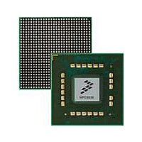
MPC8536DS Freescale Semiconductor, MPC8536DS Datasheet - Page 63

MPC8536DS
Manufacturer Part Number
MPC8536DS
Description
BOARD DEV SYSTEM MPC8536E
Manufacturer
Freescale Semiconductor
Series
PowerQUICC III™r
Type
MPUr
Datasheets
1.MPC8536EBVTAVLA.pdf
(127 pages)
2.MPC8536EBVTAVLA.pdf
(1706 pages)
3.MPC8536DS.pdf
(2 pages)
4.MPC8536DS.pdf
(126 pages)
Specifications of MPC8536DS
Contents
Board, Software and Documentation
Processor Series
MPC85xx
Core
e500
Data Bus Width
32 bit
Maximum Clock Frequency
667 MHz
Operating Supply Voltage
- 0.3 V to + 1.21 V
Maximum Operating Temperature
+ 105 C
Data Ram Size
32 KB
Interface Type
SPI, USB
Program Memory Type
DDR2, DDR3, SDRAM
Core Size
32 Bit
Program Memory Size
544KB
Cpu Speed
1.5GHz
Digital Ic Case Style
BGA
No. Of Pins
783
Supply Voltage Range
0.95V To 1.05V
Rohs Compliant
Yes
For Use With/related Products
MPC8536
Lead Free Status / RoHS Status
Lead free / RoHS Compliant
This figure shows the MII management AC timing diagram.
2.11
This section provides the AC and DC electrical specifications for the USB interface of the chip.
Freescale Semiconductor
At recommended operating conditions with OVDD is 3.3 V ± 5%.
EC_MDIO to EC_MDC hold time
EC_MDC rise time
EC_MDC fall time
Notes:
1. The symbols used for timing specifications herein follow the pattern of t
2. This parameter is dependent on the eTSEC system clock speed, which is half of the Platform Frequency (f
3. This parameter is dependent on the platform clock frequency. The delay is equal to 16 platform clock periods +/-3ns. For
5. t
6. EC_MDC to EC_MDIO Data valid t
(reference)(state)
symbolizes management data timing (MD) for the time t
invalid (X) or data hold time. Also, t
signals (D) reach the valid state (V) relative to the t
and fall times, the latter convention is used with the appropriate letter: R (rise) or F (fall).
EC_MDC output clock frequency for a specific eTSEC port can be programmed by configuring the MgmtClk bit field of chip’s
MIIMCFG register, based on the platform (CCB) clock running for the chip. The formula is: Platform Frequency
(CCB)/(2*Frequency Divider determined by MIICFG[MgmtClk] encoding selection). For example, if MIICFG[MgmtClk] = 000
and the platform (CCB) is currently running at 533 MHz, f
running at a particular platform frequency (f
maximum f
for more detail.
example, with a platform clock of 333MHz, the min/max delay is 48ns +/-3ns. Similarly, if the platform clock is 400MHz, the
min/max delay is 40ns +/-3ns).
time - Max Hold)
CLKplb_clk
Parameter/Condition
USB
is the platform (CCB) clock
MDC
for inputs and t
= f
MPC8536E PowerQUICC III Integrated Processor Hardware Specifications, Rev. 4
CCB
EC_MDIO
EC_MDIO
EC_MDC
Table 45. MII Management AC Timing Specifications (continued)
/64 and minimum f
(Output)
(Input)
Figure 35. MII Management Interface Timing Diagram
(first two letters of functional block)(reference)(state)(signal)(state)
MDDVKH
MDKHDV
Symbol
t
MDDXKH
MDC
t
t
t
MDCR
MDHF
MDCH
symbolizes management data timing (MD) with respect to the time data input
is a function of clock period and max delay time t
CCB
= f
t
MDDVKH
CCB
1
), the EC_MDC output clock frequency can be programmed between
t
MDC
MDC
/448. See the MPC8536E reference manual’s MIIMCFG register section
t
MDKHDX
clock reference (K) going to the high (H) state or setup time. For rise
MDC
Min
MDC
—
—
0
from clock reference (K) high (H) until data outputs (D) are
= 533/(2*4*8) = 533/64 = 8.3 MHz. That is, for a system
t
MDCF
(first two letters of functional block)(signal)(state)
Typ
—
—
—
t
MDDXKH
t
MDCR
for outputs. For example, t
Max
10
10
—
MDKHDX
Electrical Characteristics
. (Min Setup = Cycle
Unit
ns
ns
ns
CCB
). The actual
MDKHDX
Notes
—
—
—
63


