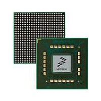
MPC8536DS Freescale Semiconductor, MPC8536DS Datasheet - Page 24

MPC8536DS
Manufacturer Part Number
MPC8536DS
Description
BOARD DEV SYSTEM MPC8536E
Manufacturer
Freescale Semiconductor
Series
PowerQUICC III™r
Type
MPUr
Datasheets
1.MPC8536EBVTAVLA.pdf
(127 pages)
2.MPC8536EBVTAVLA.pdf
(1706 pages)
3.MPC8536DS.pdf
(2 pages)
4.MPC8536DS.pdf
(126 pages)
Specifications of MPC8536DS
Contents
Board, Software and Documentation
Processor Series
MPC85xx
Core
e500
Data Bus Width
32 bit
Maximum Clock Frequency
667 MHz
Operating Supply Voltage
- 0.3 V to + 1.21 V
Maximum Operating Temperature
+ 105 C
Data Ram Size
32 KB
Interface Type
SPI, USB
Program Memory Type
DDR2, DDR3, SDRAM
Core Size
32 Bit
Program Memory Size
544KB
Cpu Speed
1.5GHz
Digital Ic Case Style
BGA
No. Of Pins
783
Supply Voltage Range
0.95V To 1.05V
Rohs Compliant
Yes
For Use With/related Products
MPC8536
Lead Free Status / RoHS Status
Lead free / RoHS Compliant
Electrical Characteristics
This figure shows the undershoot and overshoot voltages at the interfaces of the chip.
The core voltage must always be provided at nominal 1.0 V or 1.1 V. (See
Voltage to the processor interface I/Os are provided through separate sets of supply pins and must be provided at the voltages
shown in
receivers are simple CMOS I/O circuits and satisfy appropriate LVCMOS type specifications. The DDR2 and DDR3 SDRAM
interface uses differential receivers referenced by the externally supplied MV
appropriate for the SSTL_1.8 electrical signaling standard for DDR2 or 1.5-V electrical signaling for DDR3. The DDR DQS
receivers cannot be operated in single-ended fashion. The complement signal must be properly driven and cannot be grounded.
24
Table
3. The input voltage threshold scales with respect to the associated I/O supply voltage. OV
V
IH
MPC8536E PowerQUICC III Integrated Processor Hardware Specifications, Rev. 4
V
Note:
1. t
2. With the PCI overshoot allowed (as specified above), the device
IL
Figure 7. Overshoot/Undershoot Voltage for GV
B/G/L/OV
For I
For DDR, t
For eTSEC, t
For eLBC, t
For PCI, t
does not fully comply with the maximum AC ratings and device protection
guideline outlined in the PCI rev. 2.2 standard (section 4.2.2.3).
CLOCK
B/G/L/OV
2
C and JTAG, t
GND – 0.3 V
GND – 0.7 V
B/G/L/OV
refers to the clock period associated with the respective interface:
DD
CLOCK
DD
CLOCK
CLOCK
+ 20%
CLOCK
+ 5%
GND
DD
references PCI1_CLK or SYSCLK.
references MCLK.
references LCLK.
CLOCK
references EC_GTX_CLK125.
references SYSCLK.
Not to Exceed 10%
of t
CLOCK
Table 3
REF
1
n signal (nominally set to GV
for actual recommended core voltage).
DD
/OV
DD
/LV
DD
Freescale Semiconductor
DD
and LV
DD
/2) as is
DD
based


