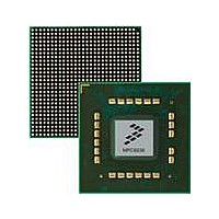
MPC8536DS Freescale Semiconductor, MPC8536DS Datasheet - Page 31

MPC8536DS
Manufacturer Part Number
MPC8536DS
Description
BOARD DEV SYSTEM MPC8536E
Manufacturer
Freescale Semiconductor
Series
PowerQUICC III™r
Type
MPUr
Datasheets
1.MPC8536EBVTAVLA.pdf
(127 pages)
2.MPC8536EBVTAVLA.pdf
(1706 pages)
3.MPC8536DS.pdf
(2 pages)
4.MPC8536DS.pdf
(126 pages)
Specifications of MPC8536DS
Contents
Board, Software and Documentation
Processor Series
MPC85xx
Core
e500
Data Bus Width
32 bit
Maximum Clock Frequency
667 MHz
Operating Supply Voltage
- 0.3 V to + 1.21 V
Maximum Operating Temperature
+ 105 C
Data Ram Size
32 KB
Interface Type
SPI, USB
Program Memory Type
DDR2, DDR3, SDRAM
Core Size
32 Bit
Program Memory Size
544KB
Cpu Speed
1.5GHz
Digital Ic Case Style
BGA
No. Of Pins
783
Supply Voltage Range
0.95V To 1.05V
Rohs Compliant
Yes
For Use With/related Products
MPC8536
Lead Free Status / RoHS Status
Lead free / RoHS Compliant
2.4.6
Please note the following FIFO maximum speed restrictions based on platform speed. The “platform clock (CCB) frequency”
in the following formula refers to the maximum platform (CCB) frequency of the speed bins the part belongs to, which is
defined in
For FIFO GMII mode:
For example, if the platform frequency is 533 MHz, the FIFO TX/RX clock frequency should be no more than 167 MHz
FIFO TX/RX clock frequency <= platform clock frequency/3.2
2.4.7
For information on the input clocks of other functional blocks of the platform such as SerDes, and eTSEC, see the specific
section of this document.
2.5
This section describes the AC electrical specifications for the RESET initialization timing requirements of the chip. This table
provides the RESET initialization AC timing specifications for the DDR SDRAM component(s).
This table provides the PLL lock times.
Freescale Semiconductor
Required assertion time of HREST
Minimum assertion time for SRESET
PLL input setup time with stable SYSCLK before HRESET negation
Input setup time for POR configurations (other than PLL config) with respect to negation of
HRESET
Input hold time for all POR configurations (including PLL config) with respect to negation of
HRESET
Maximum valid-to-high impedance time for actively driven POR configurations with respect to
negation of HRESET
HRESET rise time
Notes:
1. SYSCLK is the primary clock input for the chip.
FIFO TX/RX clock frequency <= platform clock frequency/3.2
For FIFO encoded mode:
For example, if the platform frequency is 533 MHz, the FIFO TX/RX clock frequency should be no more than
167 MHz
Table
RESET Initialization
PLL lock times
Local bus PLL
PCI bus lock time
Platform to FIFO Restrictions
Other Input Clocks
73.
MPC8536E PowerQUICC III Integrated Processor Hardware Specifications, Rev. 4
Parameter/Condition
Table 10. RESET Initialization Timing Specifications
Parameter/Condition
Table 11. PLL Lock Times
Min
—
—
—
Max
100
50
50
Min
100
100
Unit
—
—
μs
μs
μs
3
4
2
Electrical Characteristics
Max
—
—
—
—
—
5
1
Notes
—
—
—
SYSCLKs
SYSCLKs
SYSCLKs
SYSCLK
Sysclk
Unit
μs
μs
Notes
—
—
—
1
1
1
1
31


